Memory Hierarchy Design
- Chapter 2 in Computer Architecture A Quantitative Approach (6th) by Hennessy and Patterson (2017)
Ideally one would desire an indefinitely large memory capacity such that any particular… word would be immediately available… We are… forced to recognize the possibility of constructing a hierarchy of memories each of which has greater capacity than the preceding but which is less quickly accessible.
- A. W. Burks, H. H. Goldstine, and J. von Neumann, Preliminary Discussion of the Logical Design of an Electronic Computing Instrument (1946).
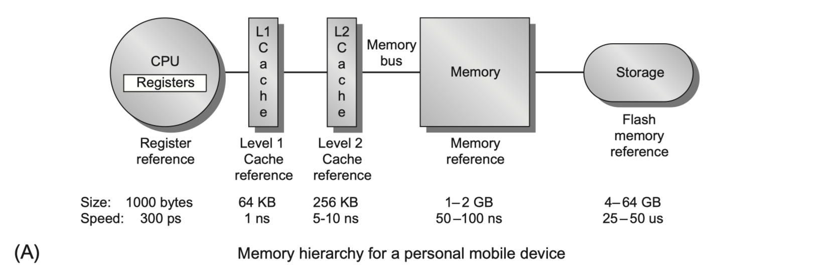
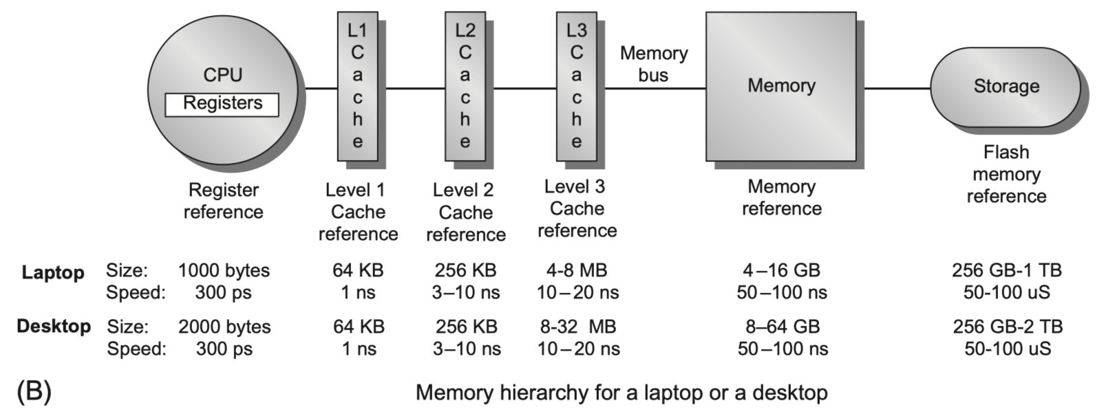
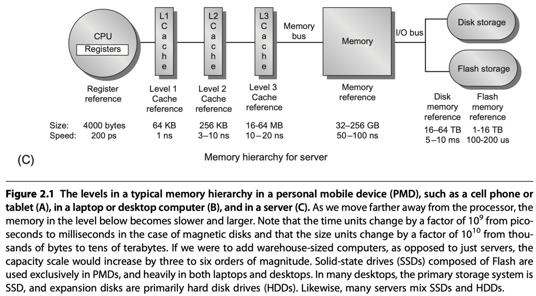
Introduction
-
Ideal case: Unlimited amounts of fast memory
-
Memory hierarchy takes advantage of
- The principle of locality
- Time and Space
- i.e. Not uniform memory access
- The trade-offs in the cost-performance of memory technologies
- Goal?
- To provide a memory system with a cost per byte that is
- Almost as low as the cheapest level of memory and
- A speed almost as fast as the fastest level.
- The principle of locality
-
Inclusion property
- In most cases (not all), the data contained in lower level are superset of the next higher level.
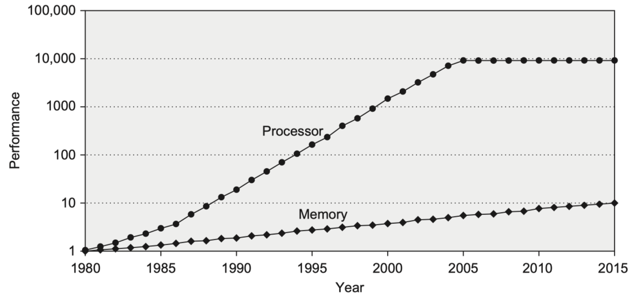
- Performance growth gap between the processors and memories $\rightarrow$ The importance of the memory hierarchy $\uparrow$
-
Multicore processors $\rightarrow$ Bandwidth requirements $\uparrow$
-
Intel Core i7 6700:
- Generates two data-memory-references/core/cycle
- With four cores and 4.2GHz clock rate
- $\rightarrow$ 32.8 billion 64-bit data references/sec = 244 GB/sec
-
- 12.8 billion 128-bit peak instruction references/sec = 191 GB/sec
- Total peak demand bandwidth = 409.6 GiB/s (?)
- Hardware solution for the high BW?
- Multi-porting and pipelining the caches
- Three levels of caches: Two private L1 and L2 per core, a shared L3
- Separate instructions and data cache at L1
- Upcoming versions use L4 DRAM cache using embedded or stacked DRAM
- DRAM BW? Only 32.1 GiB/s
- Designers focus on optimizing
- Average memory access time
- Cache access time
- Miss rate
- Miss penalty
- Power consumption
- Static power
- Dynamic power
- Average memory access time
Basics of Memory Hierarchies: A Quick Review
-
See appendix on basics on memory hierarchies $\rightarrow$ Review of Memory Hierarchy
-
Cache Basics
- Hit / Miss
- Block or line
- Spatial locality / Temporal locality
- Tag
- Where to put new block?
- Set associativity
- Direct-mapped vs n-way set associative vs fully-associative
- How to read $\rightarrow$ Easy
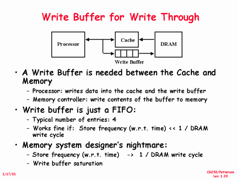
- How to write?
- Write-through: Store to memory every time
- Write-back: Store to memory when the block is replaced
- Accelerate write?
- Write-buffer: Don’t wait fully latency for memory writes
- Three Cs model for better cache design
- Compulsory: Initial fetch
- Capacity: Unable to store everything in a cache
- Conflict: If not fully-associative
- Fourth C?
- Coherency: Multithreading and multiple cores $\rightarrow$ Covered in Chapter 5
- Misses per instruction > Miss rate (Misses per memory reference)

- Better measure = Average memory access time

- Latency tolerating techniques
- Speculative processors
- Multithreading
- Six basic cache optimizations
- Larger block size to reduce miss rate
- Bigger caches to reduce miss rate
- Higher associativity to reduce miss rate
-
Multilevel caches to reduce miss penalty

- Giving priority to read misses over writes to reduce miss penalty
-
Write buffer
- RAW hazard $\rightarrow$ Solution: Check write-buffer on a read miss
-
Write buffer
- Avoiding address translation during indexing of the cache to reduce hit time
Memory Technology and Optimization
- Memory latency measures
- Access time: Time between when a read request is requested and when the desired word arrives
- Cycle time: The minimum time between unrelated requests to memory
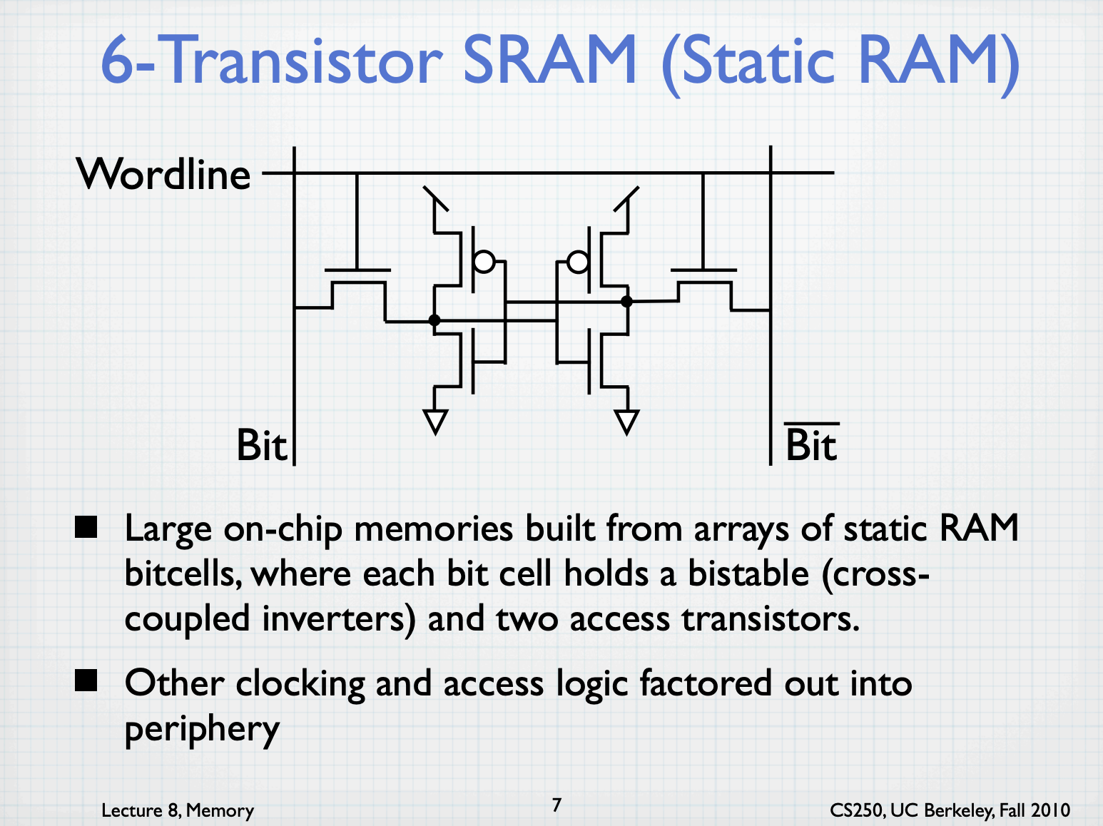
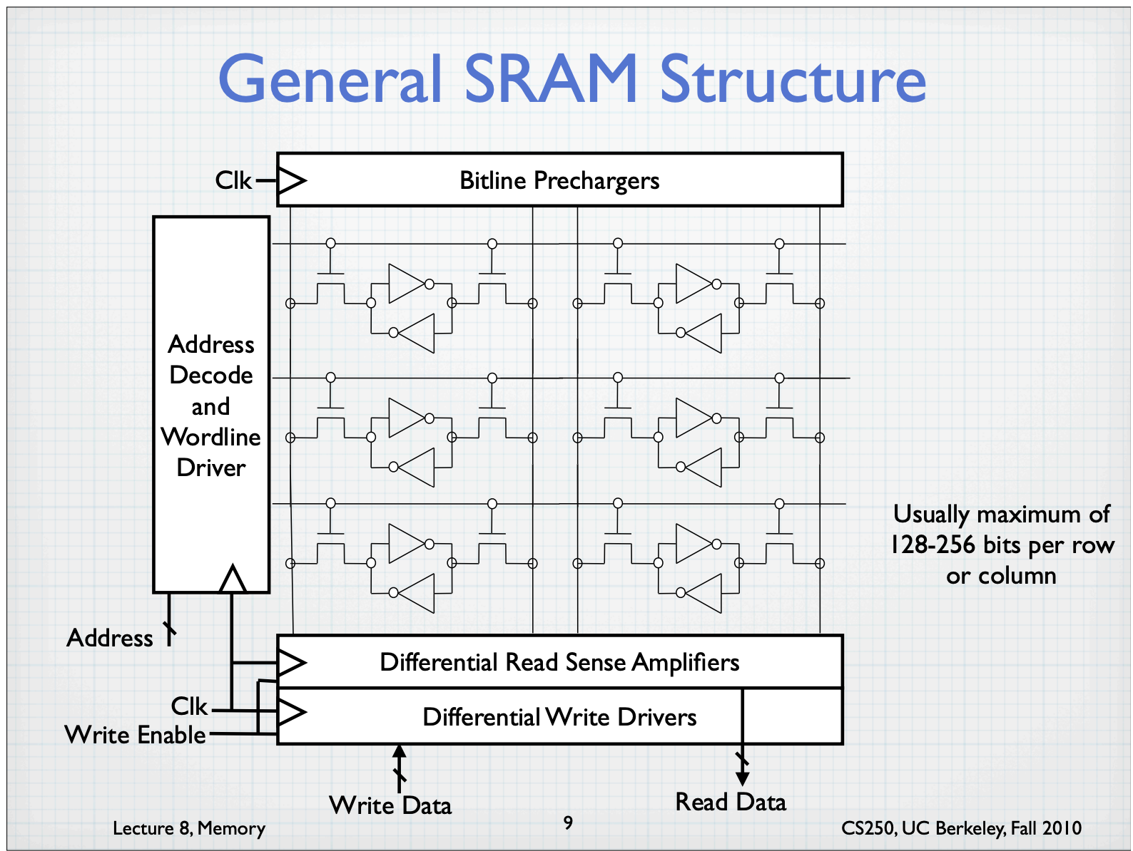
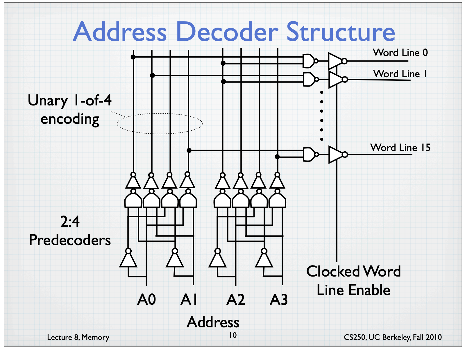
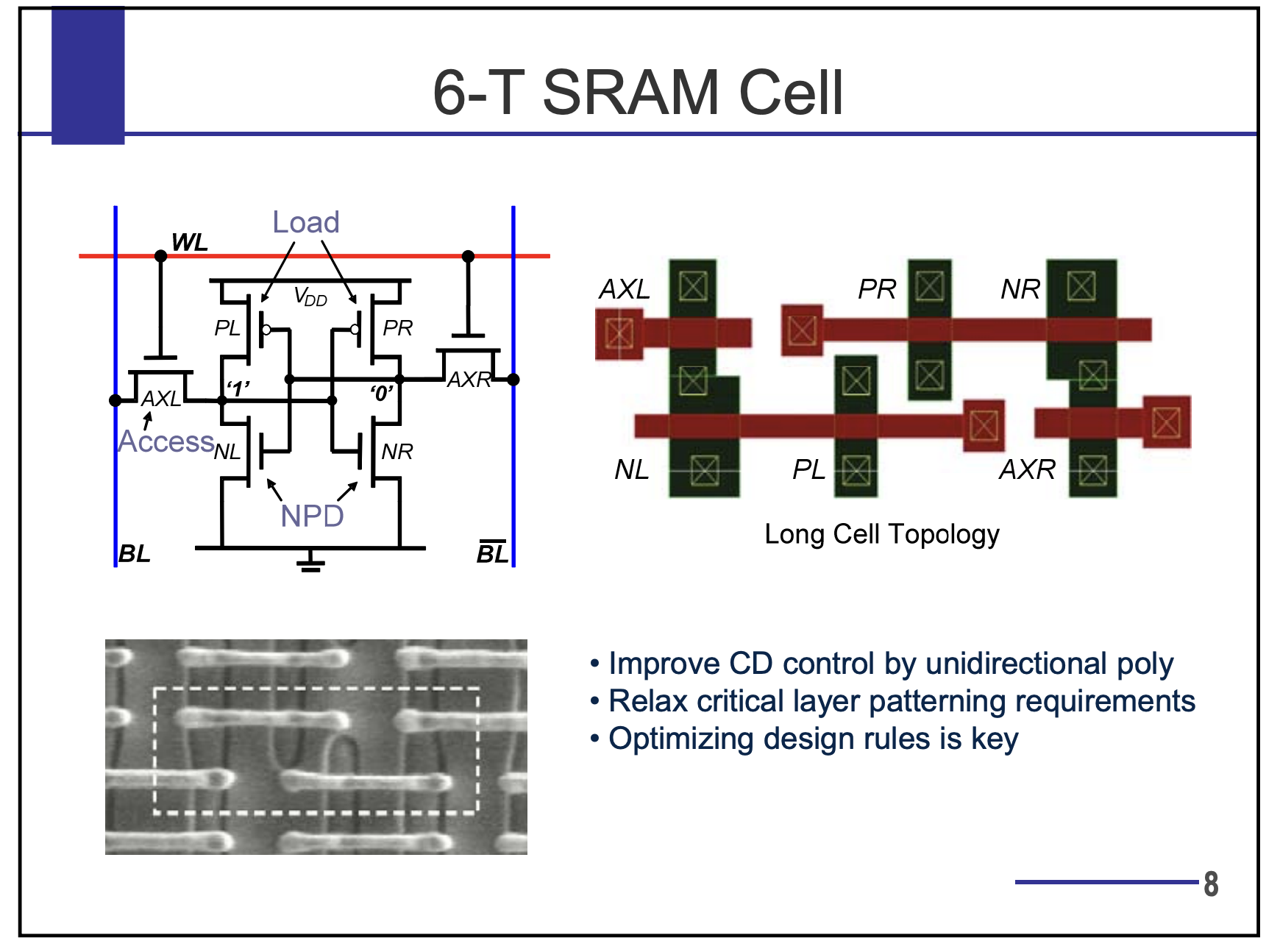
SRAM Technology
-
”Static” RAM
- Things that SRAM does not do and DRAM does
- Dynamic nature of DRAM $\rightarrow$ Data to be written back after being read
- Difference between the access time and the cycle time
- Need to refresh
-
So, in SRAM, The access time $\sim$ The cycle time
-
Typically use six transistors per bit
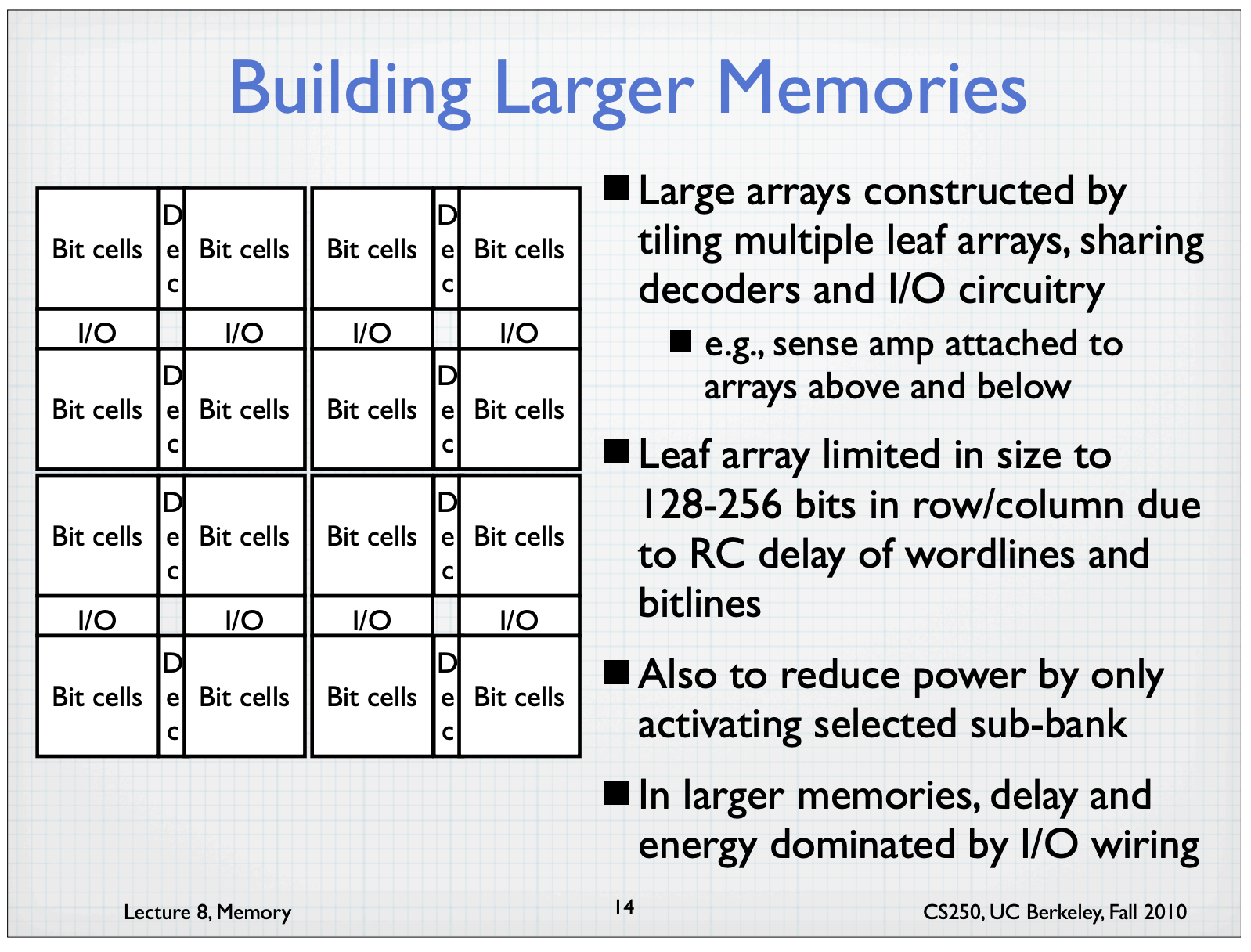
- Where to put SRAM as caches?
- Long time ago: “Separate” SRAM chips
- Recently: ”On-chip” memory
- eg. up to 60MB of cache for 24 cores w/ 128-256GB DRAM
- Access time and capacity of caches in servers?
- L1 $\rightarrow$ 1ns / 64KB
- L2 $\rightarrow$ 3-10ns / 256KB
- L3 $\rightarrow$ 10-20ns / 16-64MB
- DRAM $\rightarrow$ 50-100ns / 32-256GB
- Why is larger cache slower and power-hungry?
- Access time $\varpropto$ #Blocks in cache (except hit detection and selection in a set associative cache)
- Static power $\varpropto$ #Bits in cache
- Dynamic power $\varpropto$ #Blocks
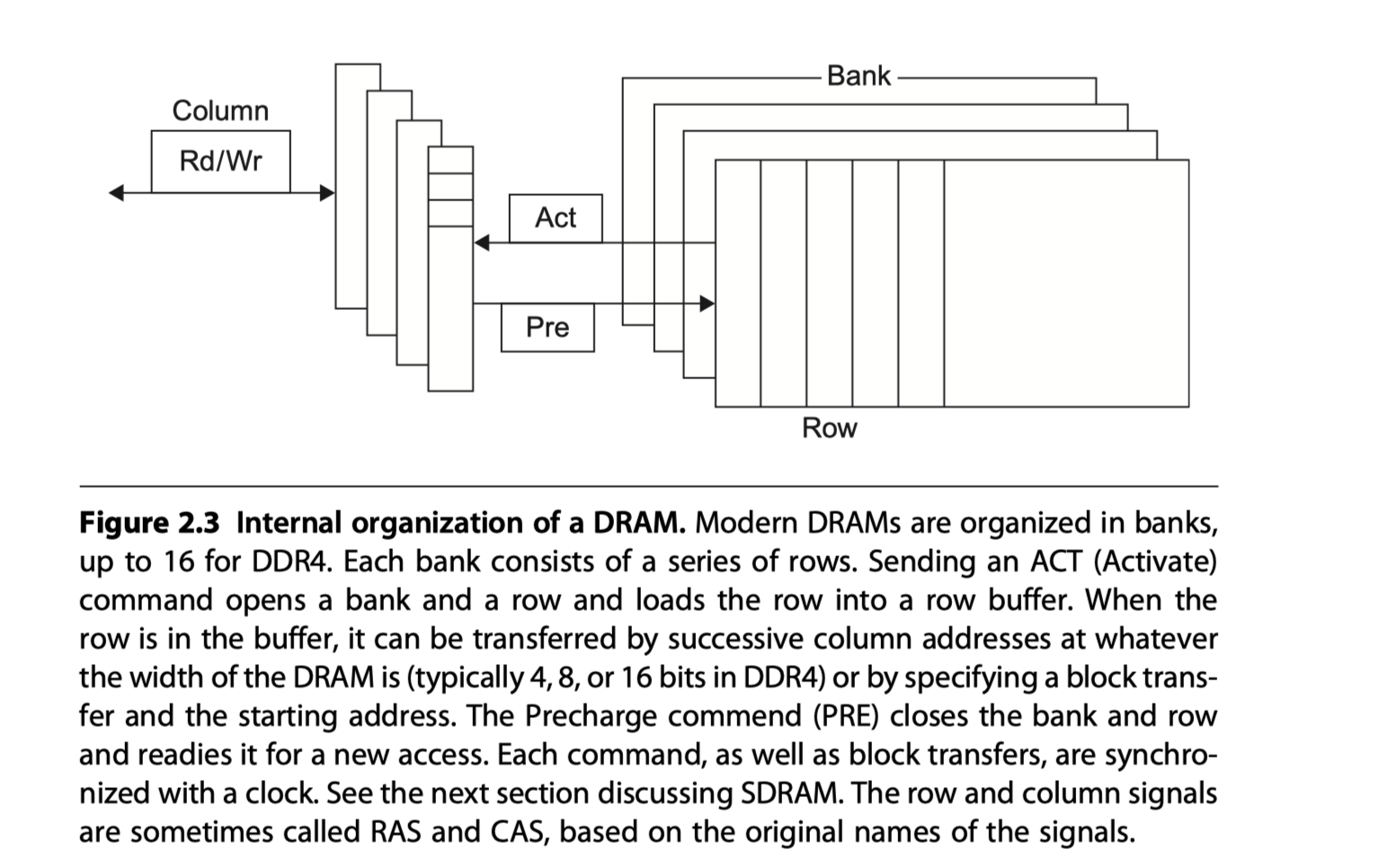
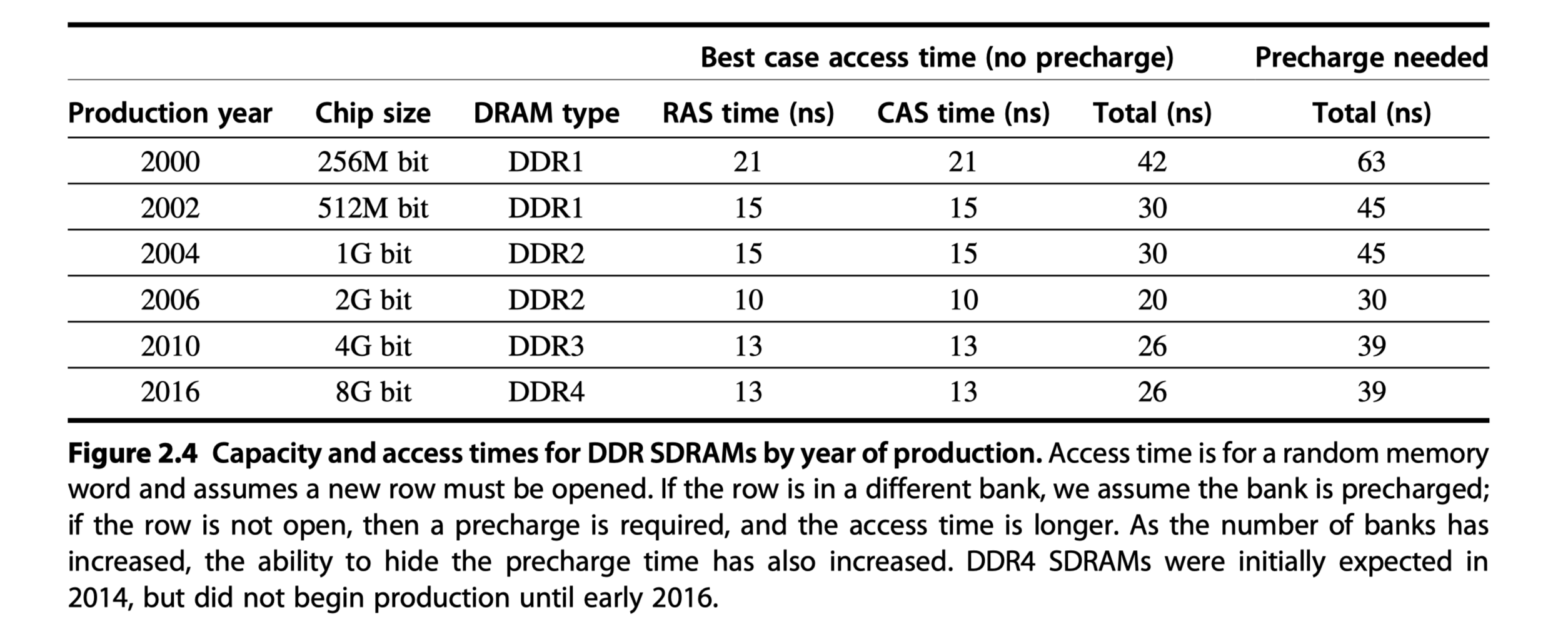
DRAM Technology
- Basic DRAM organization
- 1 Transistor = 1 Switch + 1 Capacitor
- Sensing half high charge = 1
- Sensing half low charge = 0
- Address steps
- The first half of the address
- Sent during the row access strobe (RAS)
- The other half
- Sent during the column access strobe (CAS)
- The first half of the address
- Read
- A row $\rightarrow$ A row buffer $\rightarrow$ CAS signals can select $\rightarrow$ Read out from the DRAM
- Reading a row destroys the data in the bank
- So, unused rows in the row buffer $\rightarrow$ Write back the original row position
- Refresh
- Refill the leaked charges in DRAM cells
- How?
- Reading each row and writing it back throughout all banks
- Eg. Once in a 64ms period, under 5% of the total time
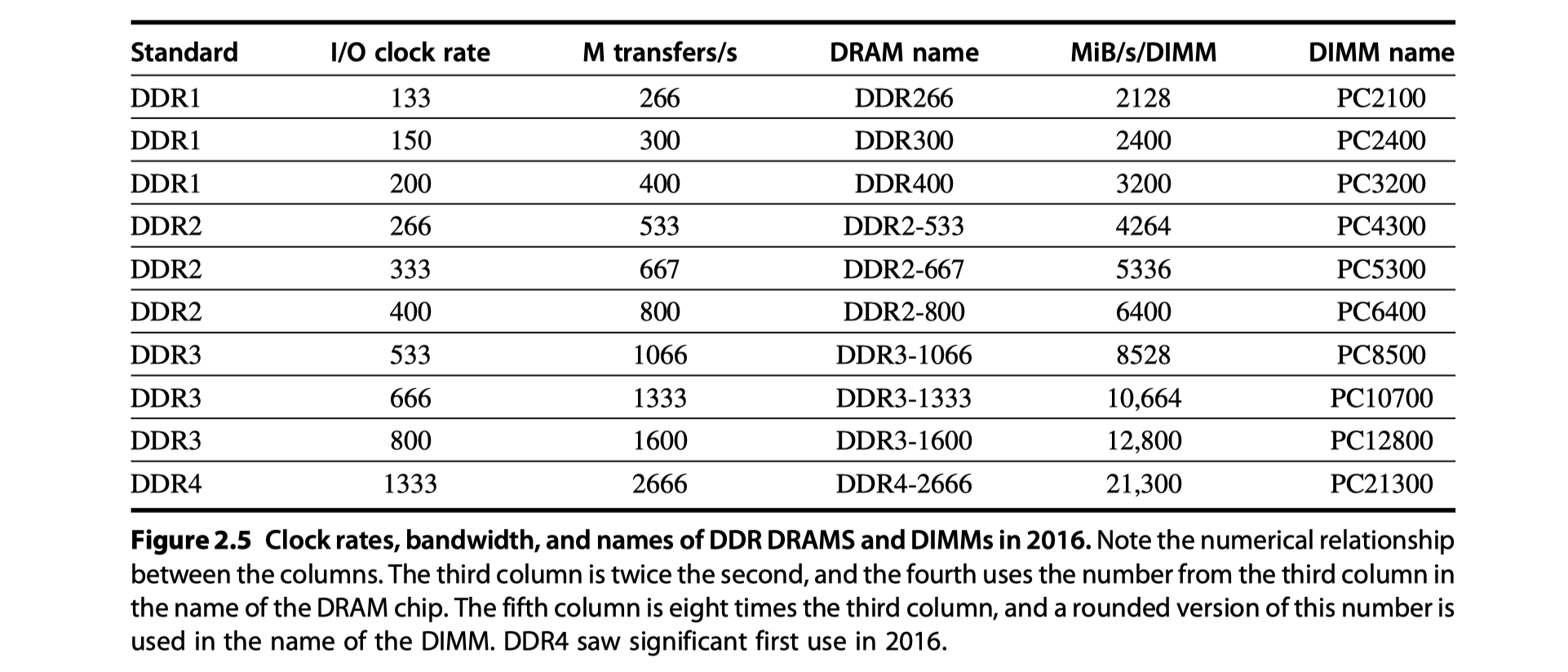
Improving Memory Performance Inside a DRAM Chip: SDRAMs
- Synchronous DRAM (SDRAM) in Mid-1990
- Before: Asynchronous interface $\rightarrow$ Overhead to synchronize with the controller
- Clock signals in the DRAM interface $\rightarrow$ Less overhead
- Burst transfer mode
- Multiple transfers without specifying a new column address
- More bandwidth
- Wider DRAMS
- DDR2, DDR3, DDR DRAMS $\rightarrow$ 4bit, 8bit, 16bit buses (?)
- Double data rate (DDR) in Early-2000
- Transfer data both on the rising and the falling edge of the memory clock
- Banks in SDRAMs
- Help with power management
- Improve access time
- Allow interleaved and overlapped access to different banks
- Address = Bank number + Row address + Column address
- New access?
- Open bank and row number (i.e. Activate = RAS) $\rightarrow$ Column address
- Sigle item request or Burst request
- After a row access, need pre-charge $\rightarrow$ Pre-charge delay for the second row access in the same bank
- Accesses of different rows in different banks can be overlapped and avoid extra pre-charge delay
- Dual Inline Memory Modules (DIMMs)
- 4-16 DRAM chips
- Normally 8 bytes wide + ECC
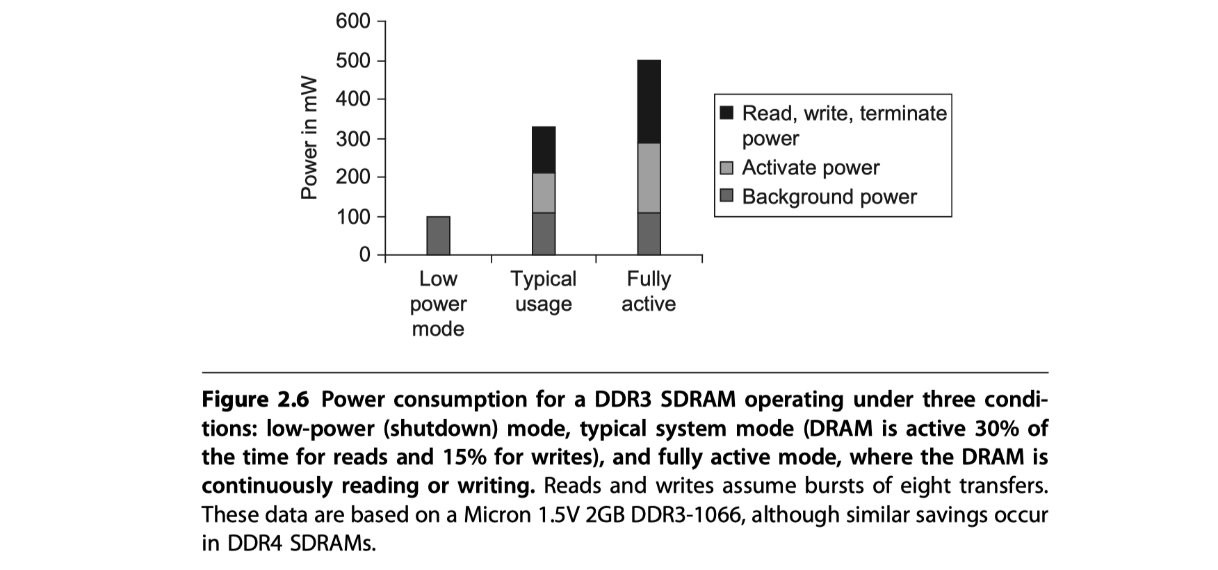
- Reducing power consumption in SDRAMs
- Low voltage (1.2V in DDR4)
- Multi-bank $\rightarrow$ Only one row in a bank is read
- Power-down mode: Ignore clock except for internal automatic refresh
Graphics Data RAMs (GDRAMs)
-
or Graphics Synchronous DRAMs (GSDRAMs)
- Special class of DRAMs based on SDRAM designs for
- Higher bandwidth of GPUs
- GDDR5 = Based on DDR3
- Previous GDDRs = Based on DDR2
- GDDRs
- Wider interfaces: 32-bits vs 4, 8, or 16 in current designs
- Higher maximum clock rate on data pins
- Connected to GPU directly
- Attached by soldering
- Not expandable array DIMMs like DRAMs
- 2-5$\times$ bandwidth per DRAM vs DDR3 DRAMs
Packaging Innovation: Stacked or Embedded DRAMs
-
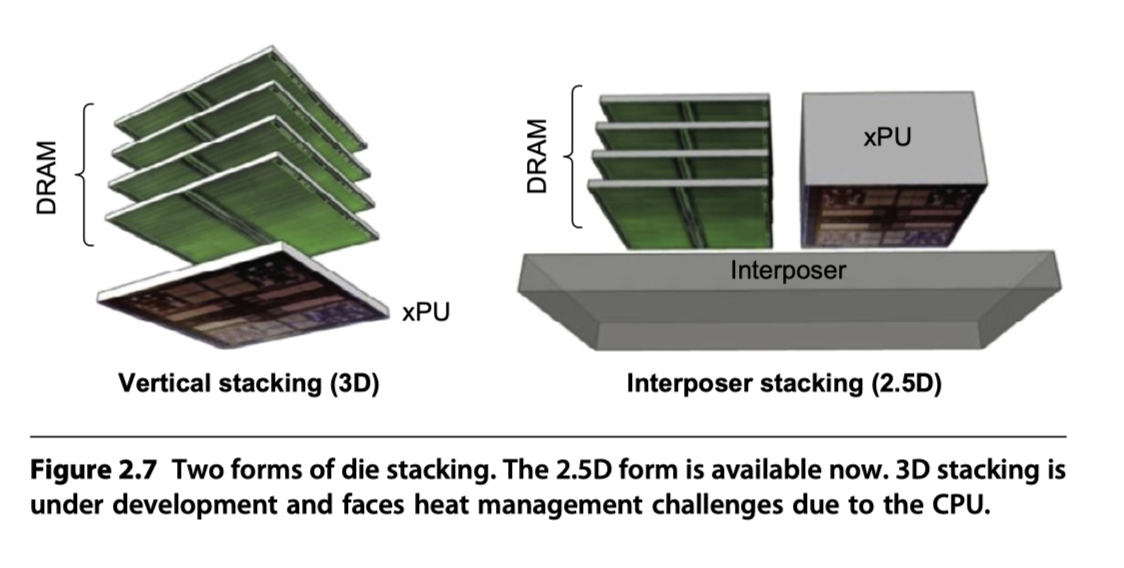
The newest innovation in 2017 = Packaging innovation
- High bandwidth memory (HBM)
- Stacked or embedded DRAM in the same package
- Lower latency
- Higher bandwidth
- Successor to GDDR5
- Method#1. 3D Technique: DRAM die directly on CPU
- Using solder bump
- Need heat management
- 8 chips, 8 GiB, 1 TB/s
- Method#2. 2.5D Technique: Stacked DRAM on a substrate
- Using interposer
Flash Memory
-
A type of EEPROM (Electronically erasable programmable read-only memory)
- NAND Flash
- Higher density than NOR Flash
- Large-scale nonvolatile memories
- Drawback
- Sequential access
- Slow writing
- Different from DRAM in
- Read
- Sequential reading
- Read entire page: 512bytes, 2KiB, 4KiB
- Speed
- Long delay for the first byte ~ 25$\mu s$
- Remainder ~ 40MiB/s
- 2KiB Transfer:
- DDR4 SDRAM = 500ns
- Flash = 75 $\mu s$ ~ 150$\times$ slower than DRAM
- Magnetic HDD = 300$\times$ slower than Flash
- Erase
- Must erase before overwrite
- Erased in blocks, not individual bytes
- 1500$\times$ slower writing than SDRAM
- 8-15$\times$ faster writing than magnetic disk
- Nonvolatile & No power consumption in standby mode
- Limited writing cycles: 100,000
- Price
- 10$\times$ Cheaper than DRAM,
- 20$\times$ more expensive than disks
- Read
- Flash Controller handles
- Remapping to redundant blocks
- Page transfer
- Caching of pages
- Write leveling
Phase-Change Memory Technology
- Use a small heating element
- To change the state of a bulk substrate
- Between its crystalline from and amorphous form
-
Each bit = Crosspoint in a 2D network = Memristor
-
Reading = Sensing the resistivity
-
Writing = Applying a current to change the phase of the material
- In 2017, Intel and Micron
- Delivered Xpoint memory based on PCM
- Much better write durability than NAND Flash
- 2-3$\times$ fast read than Flash
Enhancing Dependability in Memory Systems
- Errors during
- Fabrication process
- Dynamically during operation
- Error in
- Circuitry = Hard errors or permanent faults
- Cell’s content = Soft errors or transient faults
- Dynamic error detection
- Use error correcting codes (ECCs)
- I$ : Read only $\rightarrow$ Parity suffices
- D$ and main memory $\rightarrow$ Detect and correct
- 1-bit overhead per 8-bit data (eg. 8-bit overhead for 64-bit data)
- Chipkill
- Similar to RAID approach,
- Distributes the data and ECC information
- $\rightarrow$ A complete failure of a single memory chip can be handled !!
- Supports the reconstruction of the missing data from the remaining memory chips
- IBM, SUN, Google Cluster (Intel calls it SDDC)
- Errors in 10,000 Processors with 4GiB memories
- Parity only: ~90,000 or one unrecoverable/undetectable failure every 17 mins
- ECC only: ~3,500 or one unrecoverable/undetectable failure every 7.5 hours
- Chipkill: ~One unrecoverable/undetectable failure every 2 months!!
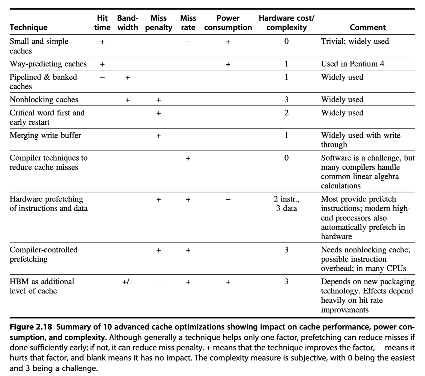
Ten Advanced Optimizations of Cache Performance
- Three metrics for cache optimization
- Hit time
- Miss rate
- Miss penalty
- Five categories of cache optimization
- Reducing the hit time
- Small and simple first-level caches
- Way-prediction
- Increasing cache bandwidth
- Pipelined caches
- Multibanked caches
- Nonblocking caches
- Reducing the miss penalty
- Critical word first
- Merging write buffers.
- Reducing the miss rate
- Compiler optimizations
- Reducing the miss penalty or miss rate via parallelism
- Hardware prefetching
- Compiler prefetching
- Reducing the hit time
#1. Small and Simple First-Level Caches to Reduce Hit Time and Power
-
Use lower levels of associativity
- Three step in the critical timing path of a cache hit
- Address the tag memory using index portion
- Compare the read tag value to the address
- (if set-associative) Setting the MUX to choose correct items
- Direct-mapped cache overlaps
- Tag check with
- Transmission of the data
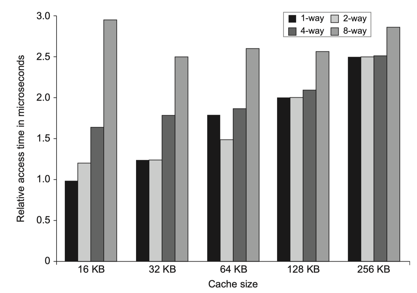
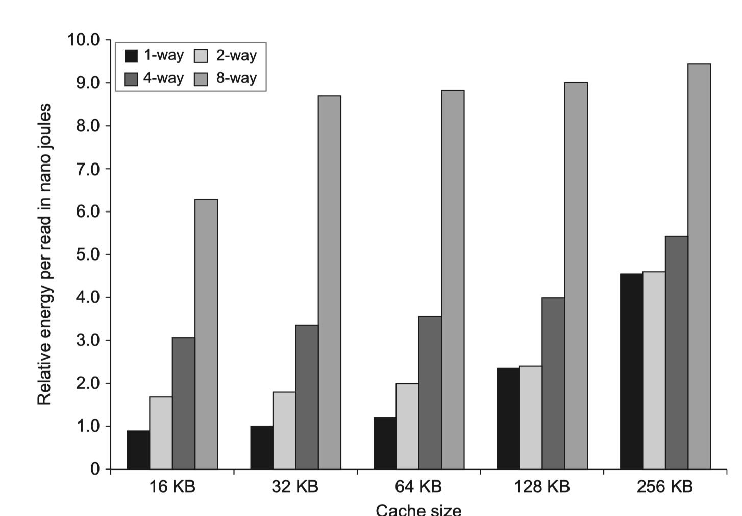
- CACTI
- Estimates hit time and power consumption
- As a function of
- Cache size
- Associativity
- #read/write ports
- More complex parameters
- Why add associativity, in recent designes?
- Increased hit-time is not big compared to > 2 clock cycles for L1$ access
- Keep TLB out of the critical path = Only virtual access to L1$ (?)
- Less conflict miss for multi-threading
#2. Way Prediction to Reduce Hit Time
-
Extra bits are kept in the cache to predict the way (or block within the set) of the next cache access.
-
This prediction means the multiplexor is set early to select the desired block, and in that clock cycle, only a single tag comparison is performed in parallel with reading the cache data.
-
A miss results in checking the other blocks for matches in the next clock cycle
-
Block predictor bits are added to each block of a cache
-
MIPS R 10000 in the mid-1990s
-
Extended form?
- Way “Selection” by using the way prediction bits to decide which cache block to actually access.
- i.e. The way prediction bits are essentially extra address bits
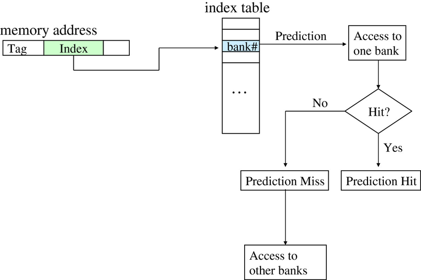
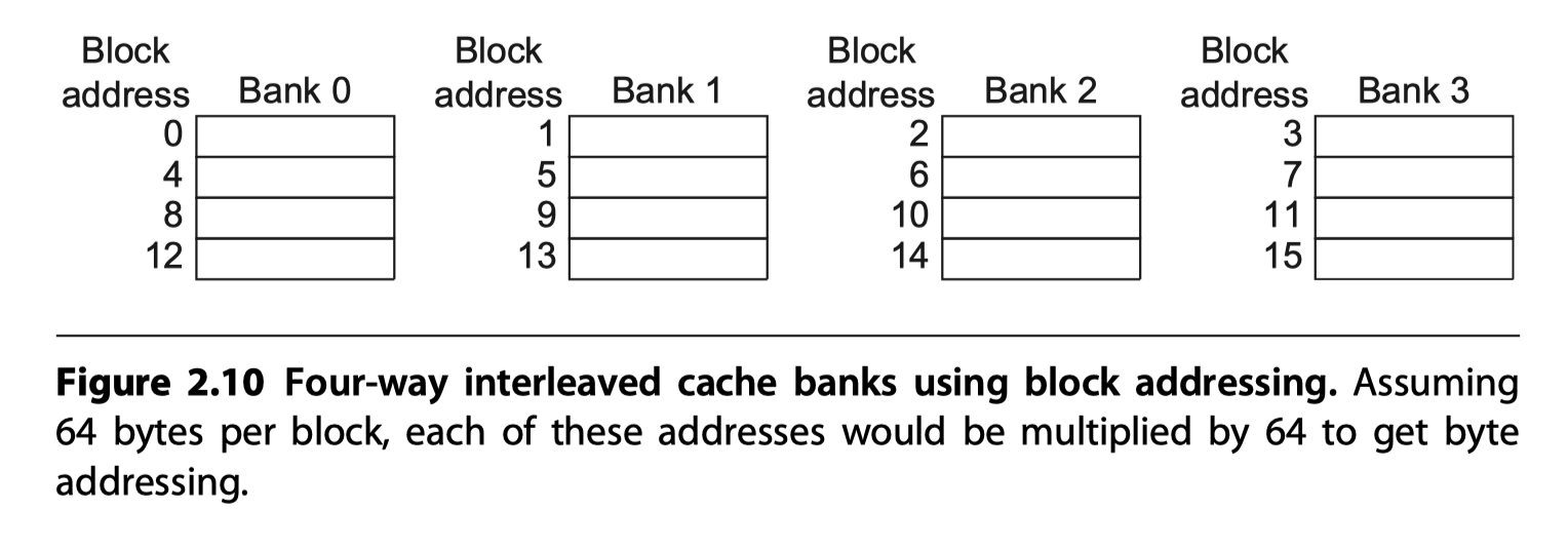
#3. Pipelined Access and Multibanked Caches to Increase Bandwidth
- To allow multiple accesses per clock
- Pipelining the cache access
- Widening the cache with multiple banks
-
Dual to the superpipelined and superscalar approaches to increasing instruction throughput
- Primarily targeted at L1$
- For instruction throughput
- Multiple banks
- Used in L2$ and L3$
- To handle multiple data cache accesses per clock,
- Divide the cache into independent banks
- Each supporting an independent access
- Intel Core i7 has four banks in L1
- To support up to 2 memory accesses per clock
- Sequential interleaving
- To spread the addresses of the block sequentially across the banks
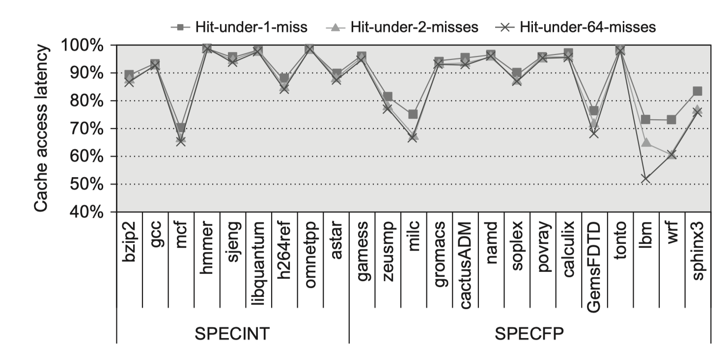
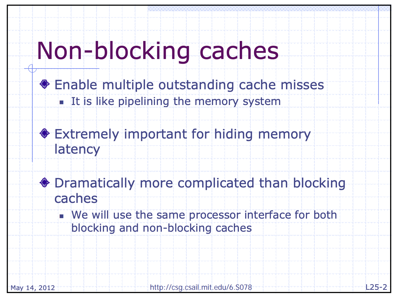
#4. Opt.: Nonblocking Caches to Increase Cache Bandwidth
- Non blocking cache = Lockup-free cache
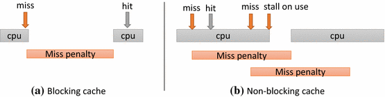
- “Hit under miss”
- Allowing the data cache to continue to supply cache hits during a miss
- “Hit under multiple misses”
- Further lower the effective miss penalty
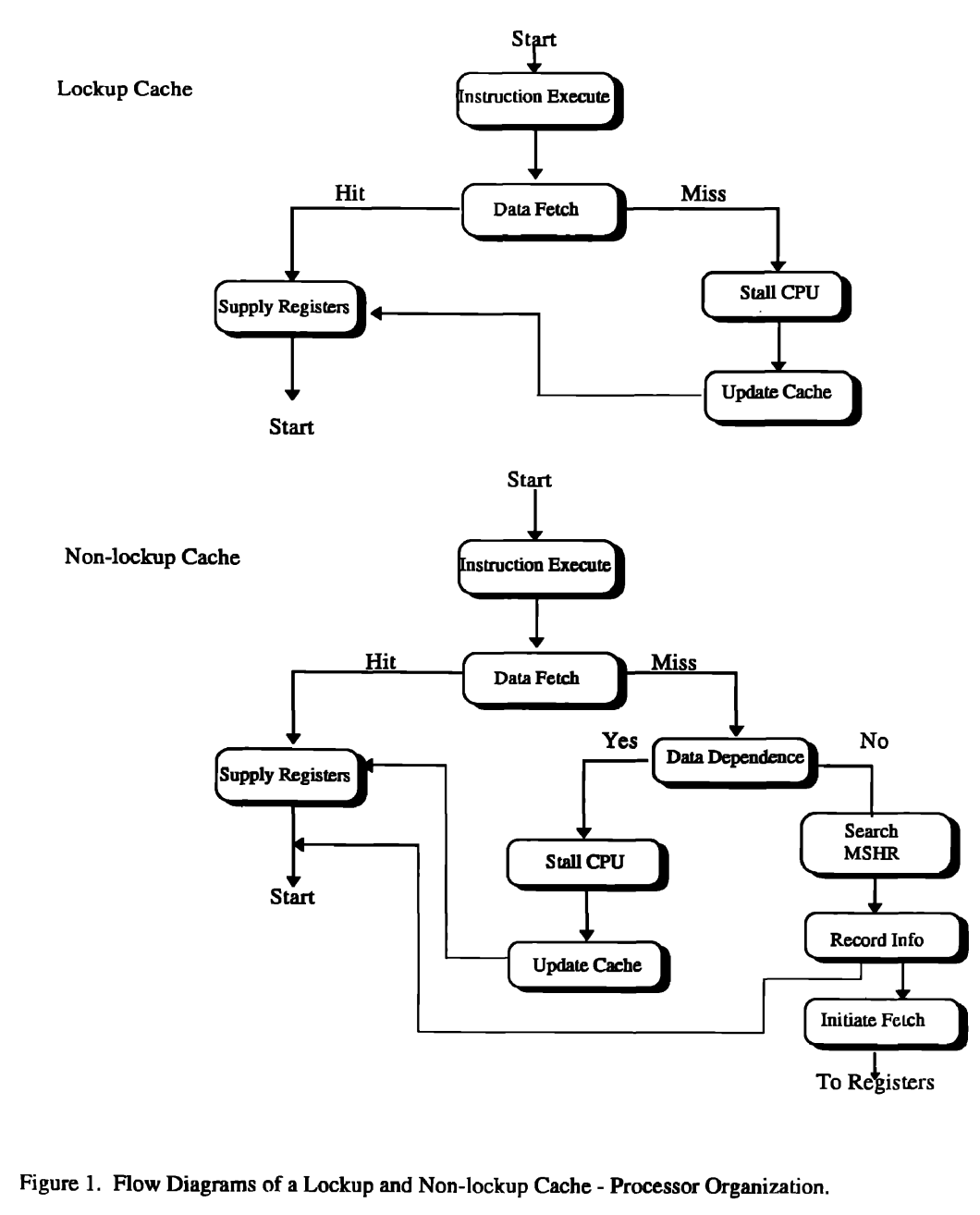
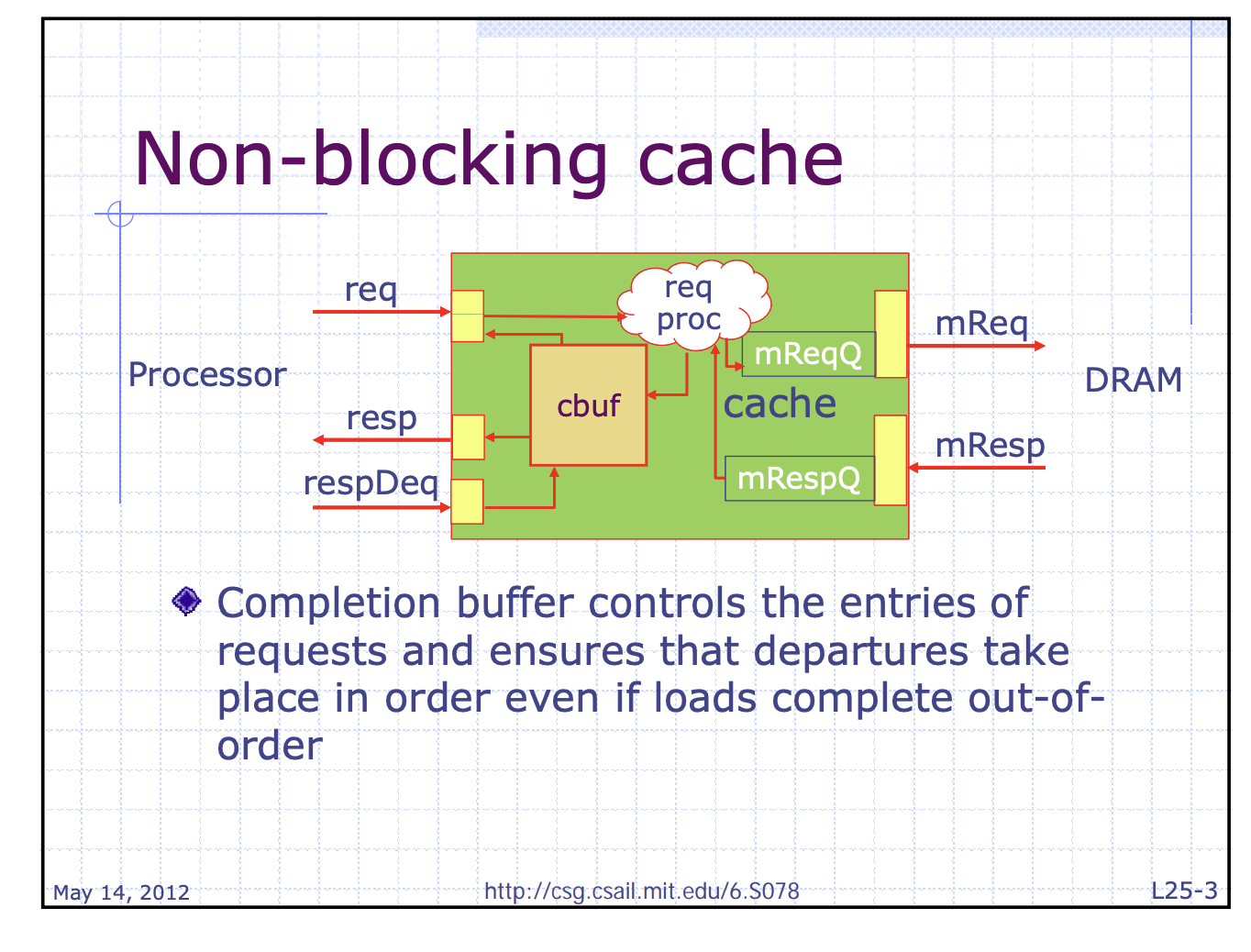
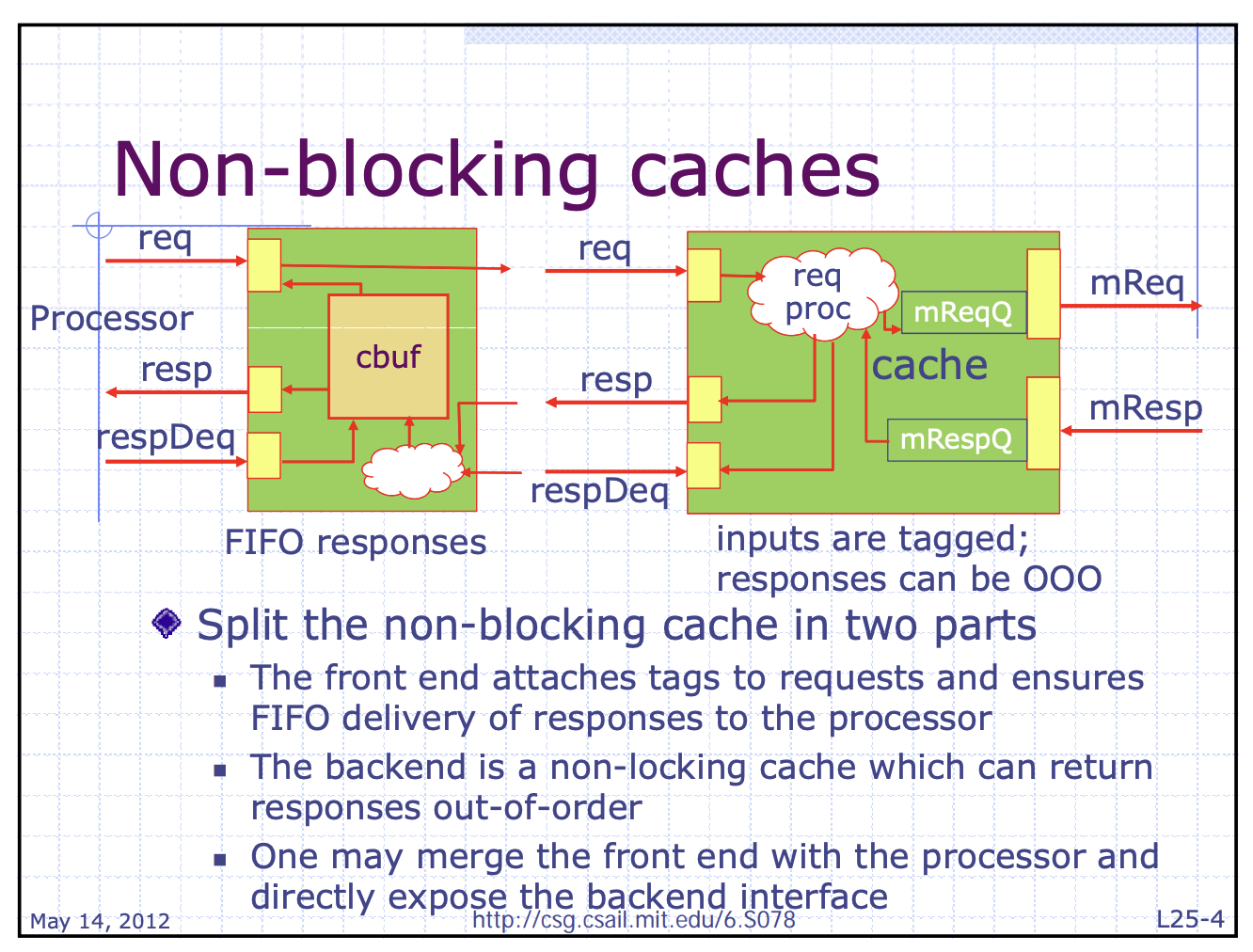
Implementing a Nonblocking Cache
- Two implementation challenges
- Arbitrating contention between hits and misses
- Hits can collide with misses returning from the next level of memory hierarchy
- Or, collision between misses
- Tracking outstanding misses $\rightarrow$ We know when loads or stores can proceed
- i.e. Sequence of the multiple missed data returning from lower memory hierarchy can be out of order!
- Must know which load or store caused the miss!
- Must know where in the cache the data should be placed!
- Miss Status Handling Registers (MSHRs) keeps tracking
- Steps
- A miss occurs
- $\rightarrow$ Allocate an MSHR
- $\rightarrow$ Enter the appropriate information about the miss
- $\rightarrow$ Tag the memory request with the index of the MSHR
- $\rightarrow$ Return data with tagged info
- $\rightarrow$ Transfer the data and tag information to the appropriate cache block
- $\rightarrow$ Notify the load or store that generated the miss
- Related to memory coherency and consistency because …
- Cache misses are no longer atomic
- i.e. the request and response are split and maybe interleaved among multiple requests
- Possible deadlock
#5. Critical Word First and Early Restart to Reduce Miss Penalty
-
Idea: Don’t wait for the full block to be loaded
- Critical word first
- Requested the missed word first from memory
- Send it to the processor as soon as it arrives
- Let the processor continue execution while filing the rest of the words in the cache block
- Early restart
- Fetch the words in normal order
- But, as soon as the requested word of the block arrives,
- Send it to the processors
- Let the processor continue execution (while filing the rest of the words in the cache block)
- Only benefits
- Designes with large cache blocks
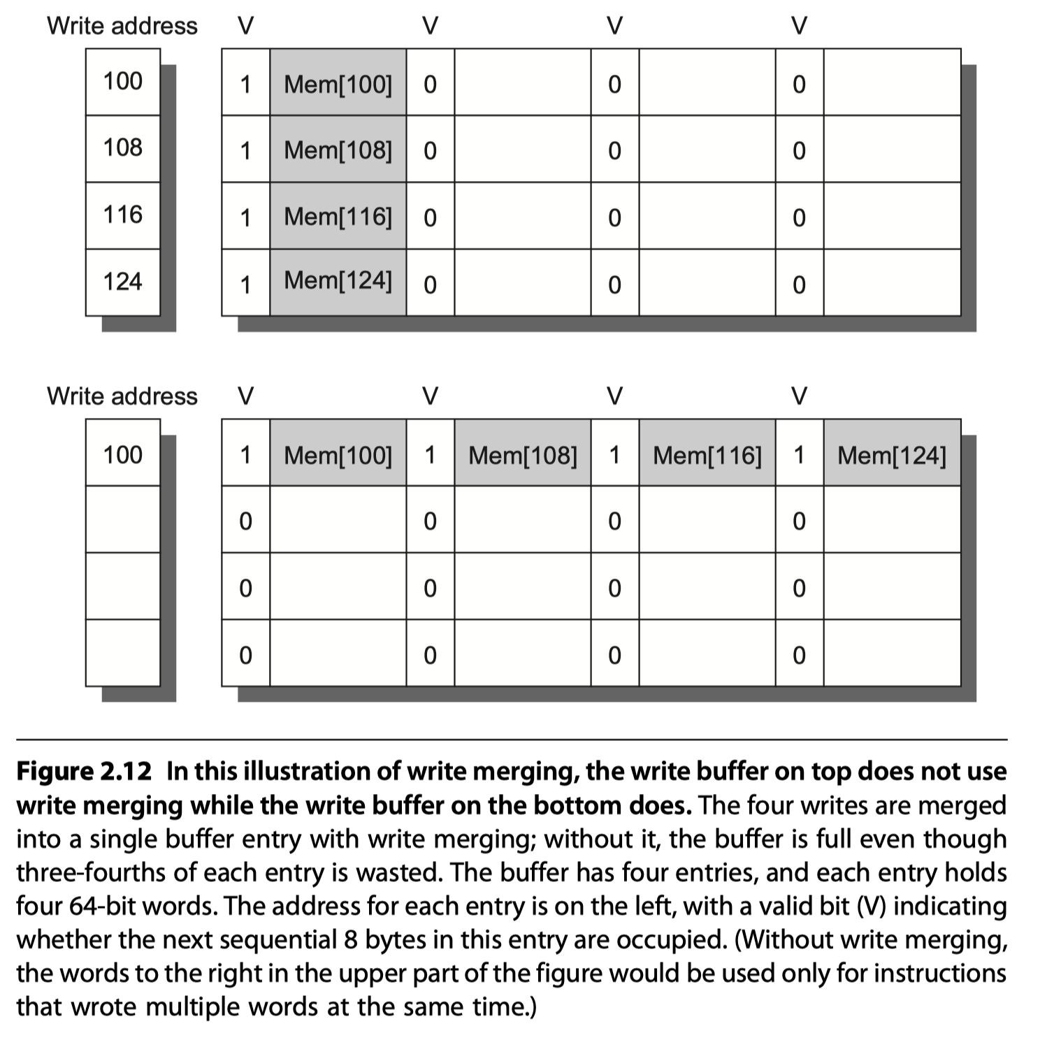
#6. Merging Write Buffer to Reduce Miss Penalty
- Write-through caches rely on write buffers
-
Write merging
- Motivation: multi-word writes usually faster than single-word writes!
- Write buffer is empty
- $\rightarrow$ The data and the full address are written in the buffer
- $\rightarrow$ The buffer is still working to send the data to memory
- $\rightarrow$ If the processor want to write new data to the address that matches the address of a valid write buffer entry
- $\rightarrow$ The new data are combined to the entry in the write buffer
- $\rightarrow$ Then, send it to memory
- Need valid bit per word!
#7. Compiler Optimization to Reduce Miss Rate
- No hardware changes
Loop Interchange
-
Programs with nested loops
-
Loop interchange can make the code access the data in the order in which they are stored
-
Reduces misses by improving spatial locality
-
Eg. $x$ = 2D-array of size [5000,100] stored in $row-major$ order
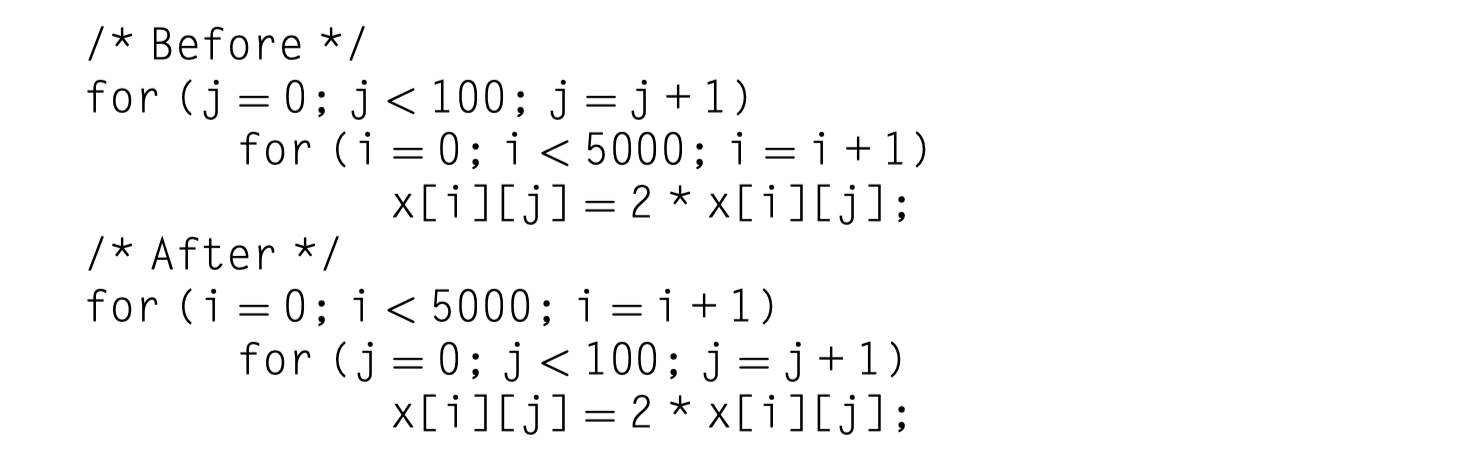
- The original code:
- Skip through memory in strides of 100 words
- The revised version:
- All the words in a block are utilized before going to the next block
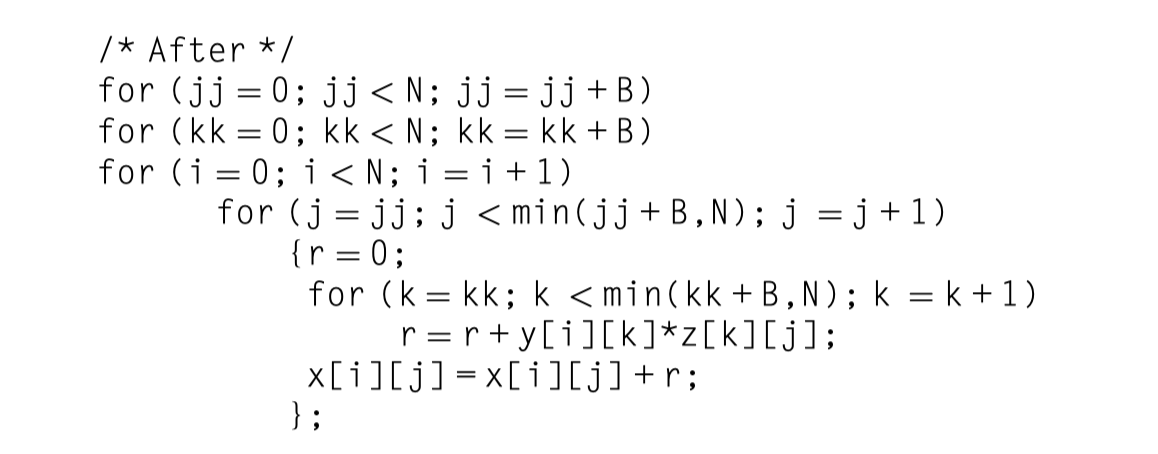
Blocking
-
Improves temporal locality to reduces misses
-
The original code: $
- x = y \times z$ GEMM
- Total memory access: $2N^3 + N^2$ without cache hit
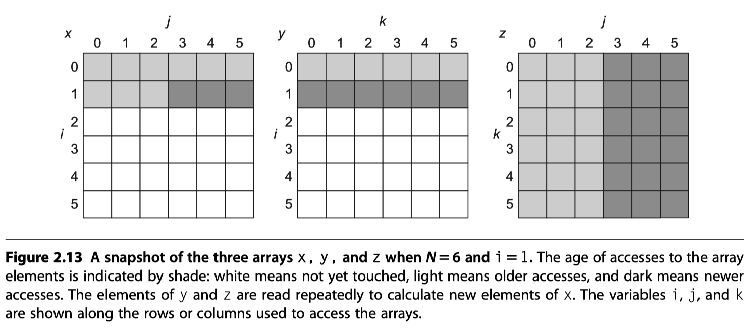
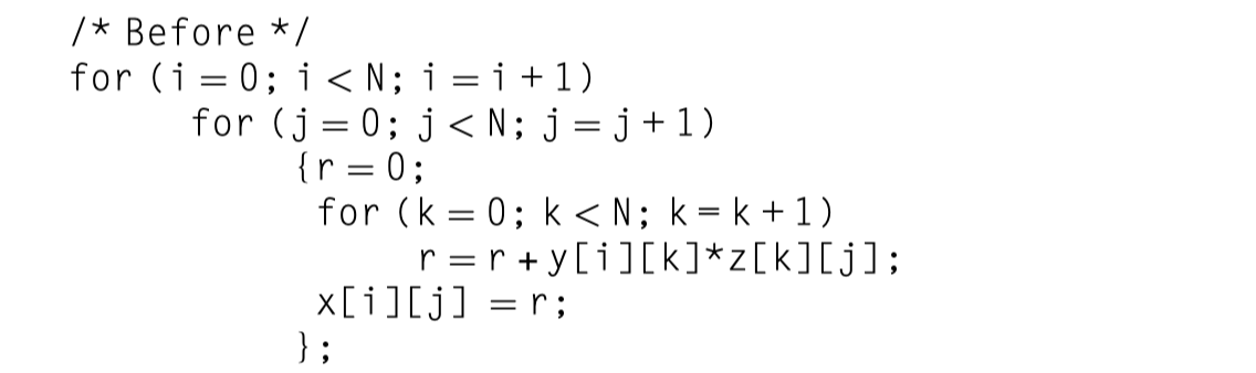
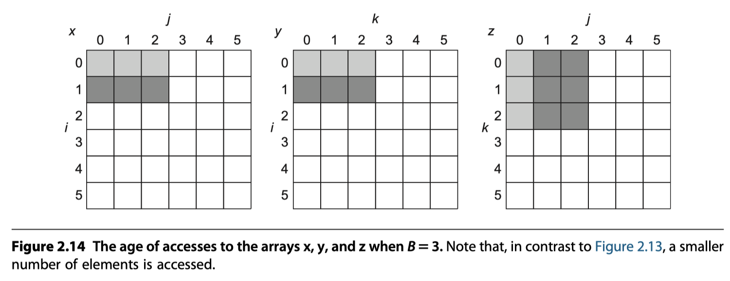
- The revised code: B
- locked with $B\times B$ = Cache size = $3\times 3^2$
- Block both $y$ and $z$ operand matrices
- Total memory access: $2N^3/B + N^2$ with cache hit
- y benefits from spatial locality (3 elements in a line)
- z benefits from temporal locality (3 time fetch from different line in the cache)
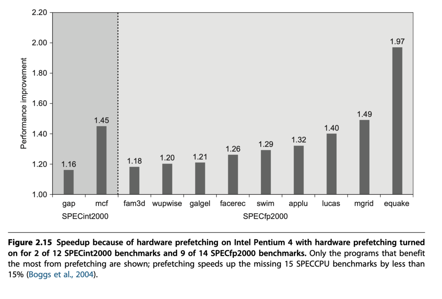
#8. Hardware Prefetching of Instructions and Data to Reduce Miss Penalty or Miss Rate
-
Prefetch items before the processor requests them!
- Instruction prefetch
- Fetch two adjacent blocks on a miss
- The requested block $\rightarrow$ Instruction cache
- The prefetched block $\rightarrow$ Instruction stream buffer
- Data prefetch
- Stream buffers that can handle either instructions or data
- 50-70% of all misses can be captured by eight stream buffers with two 64KiB four-way associative caches (One I$ and another D$)
- Intel Core i7
- Hardware prefetching into both L1 and L2
- Prefetching being accessing the next line
- More aggressive version? $\rightarrow$ Reduced performance!
#9. Compiler-Controlled Prefetching to Reduce Miss Penalty or Miss Rate
-
Alternative to hardware prefetching for the compiler?
- Goal: Overlap execution with the prefetching of data
- Loops $\rightarrow$ Unroll to prefetch data
- To insert prefetch instructions to request data
- before the processor needs it
- Flavor#1: Register prefetch
- Loads the value into a register
- Flavor#2: Cache prefetch
- Loads data only into the cache and not the register
- Faulting or Nonfaulting
- Does or does not cause an exception for
- virtual address faults and
- protection violations
- Does or does not cause an exception for
-
Normal load instruction = “faulting register prefetch instruction”
-
Nonfaulting prefetch = simply turn into no-ops if they would normally result in an exception
- “Semantically invisible” to a program
- The most effective prefetch?
- Doesn’t change the contents of registers and memory
- Cannot cause virtual memory faults
- eg. Nonfaulting cache prefetch = “nonbinding” prefetch
- Overhead?
- Instruction overhead to issuing prefetch instructions
- Example
- 8KiB direct-mapped data cache
- 16B blocks
- Write-back cache that does write allocate
- The elements of $a(3\times 100)$ and $b(101\times 3)$ = 8B : DFP

- Without prefetching
- $a$ matrix
- Spatial locality: One miss for each even values of $j$
- $3\times (100/2)=150$ misses from
- $b$ matrix
- No spatial locality: Column-wise access for row-major data arrangement
- Temporal locality: Used only twice
- $100+1 =101$ misses of $b$ matrix for operation with 0th row of $a$ matrix
- Total misses = 251
- $a$ matrix
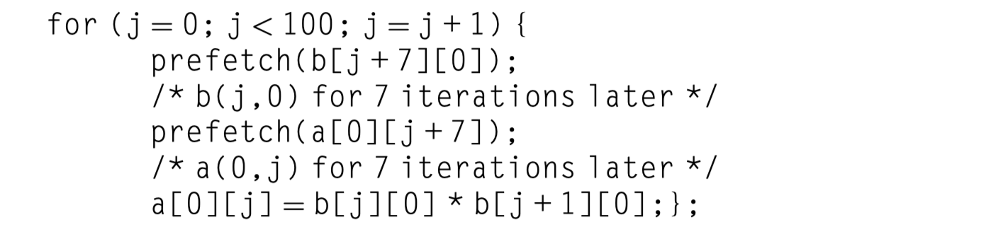
- With prefetch instruction inserted
- 7 misses for b[0][0] ~ b[6][0] in the first loop ($i=0$)
- 4 misses ($[7/2]$) for a[0][0] ~ a[0][6] in the first loop ($i=0$)
- 4 misses ($[7/2]$) for a[1][0] ~ a[1][6] in the second loop ($i=1$)
- 4 misses ($[7/2]$) for a[2][0] ~ a[2][6] in the second loop ($i=2$)
- Total misses = 19.
- Much better than the no-prefetch case.
- Trade off?
- Avoiding 232 cache miss vs Executing 400 prefetch instructions
#10. Using HBM to Extend the Memory Hierarchy
-
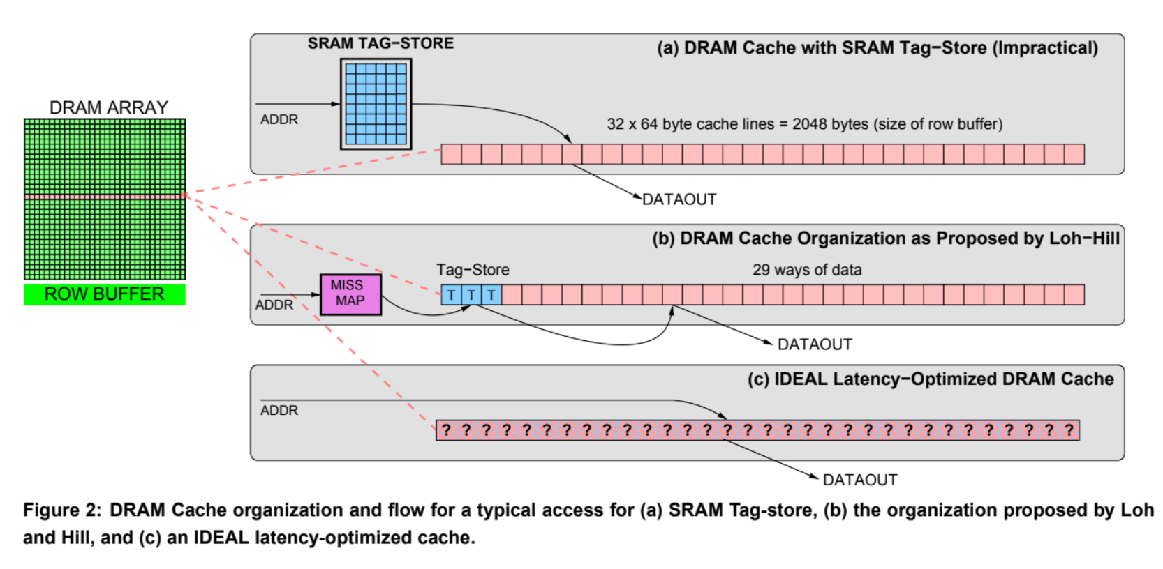
Use DRAM as a massive L4 caches
- Where do the tags reside?
- Block size = 64B?
- 1GiB L4 Cache in DRAM $\rightarrow$ 96 MiB of tags
- Too large tag size: Larger than all on-chip memory
- Block size = 4KiB?
- 1GiB L4 Cache in DRAM $\rightarrow$ 256K entries or < 1MB tags
- Acceptable tag size
- Block size = 64B?
- Problems of large 4KiB block size?
- Fragmentation problem
- Too large block size cause inefficient usage
- Contents in a block are not reused enough
- Solved by “Subblocking”.
- Subblocking allow parts of the block to be invalid
- But, doesn’t work for the second problem
- Less number of blocks
- Result in more misses
- Esp. Conflict and consistency misses
- Fragmentation problem
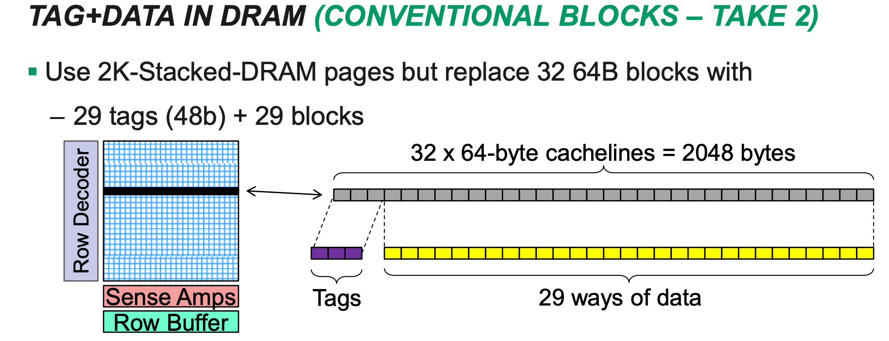
- Just store the tags inside L4 HBM?
- Two slow: Requires two accesses to DRAM for each L4 access
- One for tag
- One for data
- Solution: Place the tags and the data in the same row in the HBM SDRAM!
- Open a row only one time w/
row access - Tag check
- Data access if hit w/
column access(only 1/3 of row access)
- Open a row only one time w/
-
Loh and Hill (2011)
- L4 HBM
- Each SDRAM row
- A set of tags
- 29 data segments
- 29-way set associative cache
- Row access for tag
- Column access for data
- But, two full DRAM access for miss
-
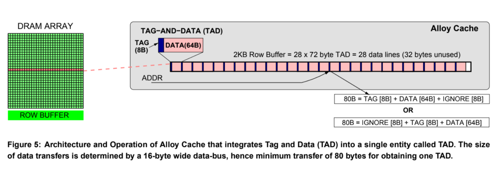
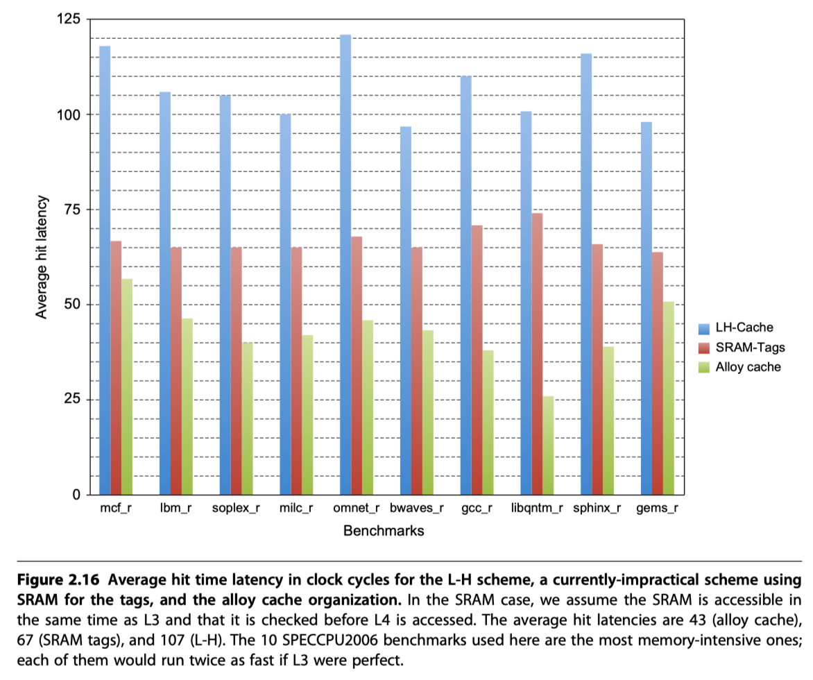
Quresh and Loh (2012)
- “Alloy cache”
- Reduces the hit time
- Molds the tag and data together and uses a direct mapped cache structure
- Directly indexing the HBM cache and doing a burst transfer of both the tag and data
- L4 access time = only a single HBM cycle!
- But, two full DRAM access for miss
- Solutions to reduce miss access time
-
- Using map that keeps track of the blocks in the cache
-
- Uses a memory access predictor that predicts likely misses using history prediction techniques
-
- Two slow: Requires two accesses to DRAM for each L4 access
Cache Optimization Summary
Virtual memory and Virtual Machines
-
Virtual machine
- An efficient, isolated duplicate of the real machine
-
Virtual machine monitor (VMM)
- VMM provides an environment for programs which is essentially identical with the original machine
- Programs run in this environment show at worst only minor decreases in speed
- The VMM is in complete control of system resources.
-
Virtual memory
- Refer to the introduction of virtual memory in Review of Memory Hierarchy
- Physical memory $\rightarrow$ Cache of secondary storage
- Move pages between the physical memory and the storage
-
TLB $\rightarrow$ Caches on the page table
- Eliminating the need to do a memory access every time an address is translated.
- Provides separation between processes that
- Share one physical memory
- But have separate virtual address spaces
-
Protection and privacy between processes sharing the same processor
- Electronic burglaries
- Arise from programming errors that allow a cyberattack
Protection via Virtual Memory
-
Page-based virtual memory,
- Including a TLB that caches page table entries,
- Is the primary mechanism that protects processes from each other.
- Protection via segmentation and paging in the 80x86
- Refer to Sections B.4 and B.5 in Review of Memory Hierarchy for more detailed description
-
Multiprogramming, where several programs running concurrently share a computer,
- Has led to demands for protection and sharing among programs
- And to the concept of a process
- A process
- “Breathing air and living space of a program”
- Must be possible to switch from one process to another.
- i.e. Process switch or context switch
-
OS and architecture join forces to
- Allow processes to share the hardware
- Yet not interfere with each other
Role of architecture for protection?
- Provide at least two modes to distinguish …
- User process
- Operating system process = Kernel process = Supervisor process
- Provide a portion of the processor state
- that a user process can use but not write.
- This state includes
- User/Supervisor mode bit
- Exception enable/disable bit
- Memory protection information
- Provide mechanism to switch the processor modes
- User mode $\rightarrow$ Supervisor mode : System call
- Implemented as a special instruction
- Transfer control to a dedicated location in supervisor code space
- Save the PC from the point of the system call
- Supervisor mode $\rightarrow$ User mode :
- Like a subroutine return,
- Restore the previous/user mode
- User mode $\rightarrow$ Supervisor mode : System call
- Provide mechanisms to limit memory accesses
How to implement protection?
-
Add protection restrictions to each page of virtual memory
- The protection restrictions included in each page table entry determines …
- whether a user process can read this page,
- whether a user process can write to this page, and
- whether code can be executed from this page
- neither read nor write a page if it is not in the page table.
-
Because only the OS can update the page table,
-
The paging mechanism provides total access protection.
- Paged virtual memory access
- At least twice longer latency
- One for obtaining the physical address
- Need to look up a huge page table!
- One for getting the data
- Solution of the slow paged virtual memory access
- Rely on the principle of locality
- If the access has locality, then the address translation have locality
- $\rightarrow$ Use Translation lookaside buffer (TLB)
- i.e. Use a special cache for page table
- Exploiting locality in memory hierarchy?
- Cache $vs$ Main-memory
- Page $vs$ Virtual-memory
- TLB $vs$ Page-table
- TLB entry or Page-table entry
- Mapping between the virtual address and the physical address of a page
-
Tag-portion:
- Holds portions of the virtual address
-
Data-portion:
- Holds a physical page address, protection field, valid bit, and usually a use bit and a dirty bit.
- How to update a page table entry?
- OS update the values in the page table
- Invalidating the corresponding TLB entry
- Is it enough to let your computer architecture obey the restrictions on pages?
- Not enough!!
- We depend on the operating system as well as the hardware!
- What’s the problem of OS?
- It is too big to find and fix the bugs in it
- 10s of millions of lines
- Bug rate (?) = One per thousand lines
- So much security hole
- Solution? Use a protection model like virtual machines with a much smaller code base than the full OS
Protection via Virtual Machines
-
First developed in the late 1960s
- Why virtual machines?
- Importance of isolation and security
- Failures in security and reliability of standard OSs
- Sharing of a single computer among many users
- Overhead of VMs become acceptable
- Definition of VMs?
- “All emulation methods that provide a standard software interface”
- Our focus here will be on VMs where the ISA presented by the VM and the underlying hardware match
- i.e. System virtual machines
- e.g. IBM VM/370, VMware ESX Server, Xen
-
With a VM, multiple OSes all share the hardware resources
-
Virtual machine monitor (VMM) or Hypervisor
- Underlying hardware = ’Host’
- Host’s resources are shared among the ’Guest’ VMs
- VMM determines how to map virtual resources to physical resources
- Time-shared
- Partitioned
- Emulated in software
- Much smaller than a traditional OS
- Isolation portion of a VMM ~ only 10,000 lines of code
- Cost of virtualization?
- User level processor-bound programs $\rightarrow$ Little OS invocation $\rightarrow$ Little virtualization overhead
- I/O-intensive workloads $\rightarrow$ Many system calls and privileged instructions $\rightarrow$ OS-intensive $\rightarrow$ High virtualization overhead
- Slowed down by the instructions that must be emulated by the VMM
-
If Guest ISA = Host ISA $\rightarrow$ Run instructions directly on the native hardware
- VM’s benefits
- Protection improvement
- Manage software
- Free to use multiple/old/new/legacy OSes
- Mange hardware
- Multiple software stacks share hardware
- Possible to migrate ‘running VM’ to a different computer
- Basic requirement of system virtual machines
- System mode and user mode (at least)
- A privileged subset of instructions
- Available only in system mode
Requirements of a Virtual Machine Monitor
- VMMs that present a software interface to guest software
- Must isolate the state of guests from each other
- Must protect itself from guest software (including guest OSes).
- VMM must control everything
- access to privileged state
- address translation
- I/O
- exceptions and interrupts
- Privilege level of VMM > Guest VMs
Instruction Set Architecture Support for Virtual Machines
-
Virtualizable architecture
- VM planning during the design of the ISA $\rightarrow$
- Allows the VM to execute directly on the hardware
- e.g. IBM 370, recent x86, RISC-V
-
Privileged instruction by guest OS?
- Trap to VMM $\rightarrow$ Support a virtual version of the sensitive information as the guest OS expects
- No VMM trapping support? $\rightarrow$
- Special precautions by VMM,
- Locate all problematic instructions
-
Multi-level privileged instructions
- One for guest user
- One for some OS operations that
- exceed the permissions granted to a user program
- But, do not require intervention by VMM because they cannot affect any other VM
- One for VMM
- eg. Xen design
Impact of Virtual Machines on Virtual Memory and I/O
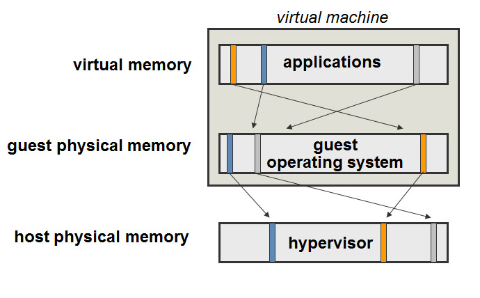
- Virtualization of virtual memory
- Each guest OS in every VM …
- manages its own set of page tables
- Separation of the notion of real and physical memory!
- Real memory?
- Intermediate level between virtual memory and physical memory
- Virtual memory $\rightarrow$ Real memory
- Mapped by guest OS
- Via page tables
- Guests’ real memory $\rightarrow$ Physical memory
- Mapped by VMM page tables
- Real memory?
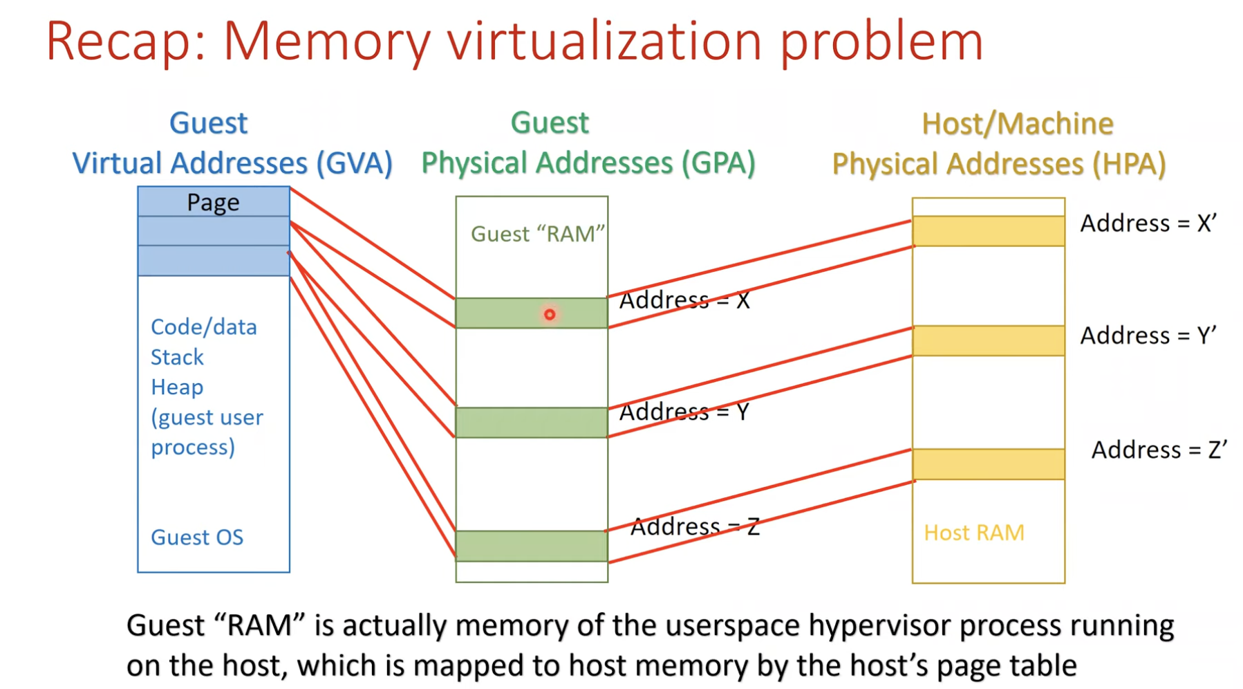
- Memory virtualization and VMware Ballooning by FRANKBRIX
- Inside a virtual machine you start an application. For instance solitaire
- Solitaire as an application will ask the guest operating system (in this case windows) for memory. Windows will give it memory and map it from the virtual memory $\rightarrow$ guest physical memory (real memory in H&P)
- What happens next is that the hypervisor sees the request for memory and the hypervisor maps guest physical memory (real memory in H&P) $\rightarrow$ host physical memory (physical memory in H&P)
- Now everything is perfect. You play solitaire for a few hours. And then you close it down.
- When you close solitaire the guest operating system will mark the memory as “free” and make it available for other applications. BUT since the hypervisor does not have access to Windows’ “free memory” list the memory will still be mapped in “host physical memory” and putting memory load on the ESXi host.
- This is where ballooning comes into place. In case of an ESXi host running low on memory the hypervisor will ask the “balloon” driver installed inside the virtual machine (with VMware Tools) to “inflate”
- The balloon driver will inflate and because it is “inside” the operating system it will start by getting memory from the “free list”. The hypervisor will detect what memory the balloon driver has reclaimed and will free it up on the “host physical memory” layer!
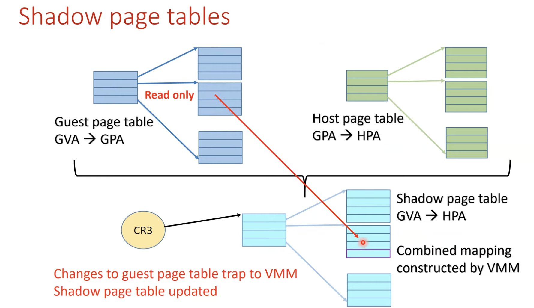
- Shadow page table (SPT)
- Double mapping is too expensive
- SPT maps directly (!) from
- the guest virtual address space
- to the physical address space of the hardware
- How to?
- VMM detects all modification to the guest’s page table
- Ensure the shadow page table entries being used by the hardware for translations
- So, VMM must trap any attempt by the guest OS
- to change ints page table or
- to access the page table pointer
- I/O Virtualization?
- Most difficult part of system virtualization
- Increasing number of I/O devices
- Increasing diversity of I/O device types
- Sharing of a real device among multiple VMs
- Supporting the myriad of device drivers
- How to?
- Giving each VM generic version of each type of I/O device driver
- Then, VMM handle real I/O
- eg1. HDD $\rightarrow$ virtual tracks/sectors
- eg2. Network $\rightarrow$ VMs share short time slices
Extending the Instruction Set for Efficient Virtualization and Better Security
- Two primary areas of performance improvement
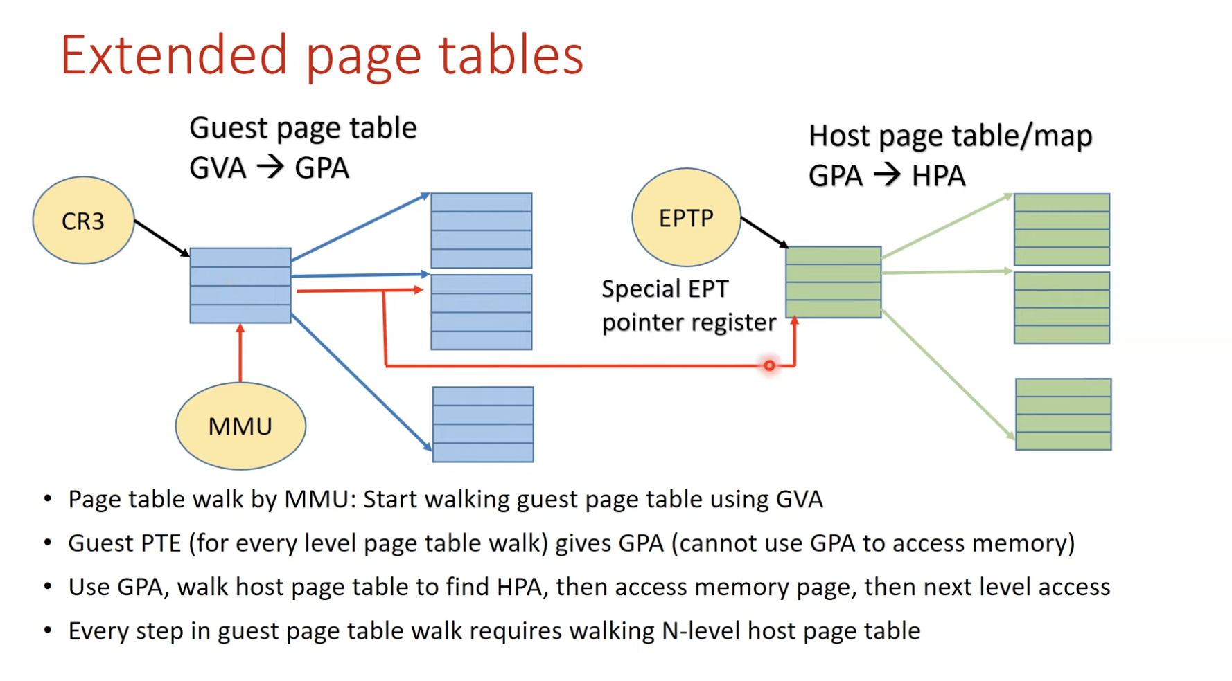
- Handling page tables and TLBs (the cornerstone of virtual memory)
- Avoiding unnecessary TLB flushes
- Using the nested page table mechanism (eg. IBM)
- Rather than a complete set of shadow page tables
- I/O, specifically handling interrupts and DMA.
- Allow a device to directly use DMA to move data (eliminating a potential copy by the VMM)
- Allow device interrupts and commands to be handled by the guest OS directly.
- Handling page tables and TLBs (the cornerstone of virtual memory)
- Concerns about security
- VMM penetration followed by memory remapping to access to the credit card information data
- Trojan horse in the same VM with the credit card information data
- eg. Intel’s software guard extensions (SGX)
- Allow user programs to create “enclaves”
- Enclaves: Portions of code and data that are always encrypted and decrypted only on use and only with the key provided by the user code.
An Example VMM: The Xem Virtual Machine
- VM developers decided to
- Allow the guest OS to be aware that it is running on a VM
- Para-virtualization in Xen VMM
- Allowing small modification to the guest OS to simplify virtualization
- Xen VMM
- Used in Amazon’s web services data centers
- Provides a guest OS with a virtual machine abstraction
- eg1. Avoid flushing the TLB
- eg2. Allow the guest OS to allocate page, checking protection restriction
- Four protection level
- Lv 0: Xen VMM
- Lv 1: Guest OSs
- Lv 3: Applications
- Xen modifies the guest OS
- Not to use problematic portions of the architecture
- eg. Change 1% (~3000 lines) of 80x86 specific code in Linux port to Xen
- Driver domains
- Special privileged VMs to simplify the I/O challenge of VMs
- Run the physical device drivers
- Regular VMs (guest domains) run simple virtual device drivers that must communicate with the physical device drivers in the driver domains
- Data communication between guest and driver domains $\rightarrow$ Done by page remapping
Cross-Cutting Issues: The Design of Memory Hierarchies
(Topics from other chapters that are fundamental to memory hierarchies)
Protection, Virtualization, and Instruction Set Architecture
-
IBM360 $\rightarrow$ IBM370 : Support virtual memory
-
80x86 instruction
POPFproblem -
IBM mainframe hardware and VMM’s 3 steps to improve performance
- Reduce the cost of processor virtualization.
- Reduce interrupt overhead cost due to the virtualization.
- Reduce interrupt cost by steering interrupts to the proper VM without invoking VMM.
Autonomous Instruction Fetch Units
-
OoO or deep pipeline processors decouple the instruction fetch using a separate instruction fetch unit
-
The instruction fetch unit accesses the instruction cache to fetch an entire block before decoding it into individual instructions
-
May generate additional misses, but may reduce the total miss penalty incurred
-
Also include data prefetching
Speculation and Memory Access
- Speculation
- An instruction is tentatively executed before the processor knows whether it is really needed.
- Rely on branch prediction
- If incorrect, flush the speculated instructions from the pipeline
- Protection with speculation?
- With speculation, the processor may generate memory references, which will never be used because the instructions were the result of incorrect speculation. Those references, if executed, could generate protection exceptions. Obviously, such faults should occur only if the instruction is actually executed.
Special Instruction Caches
- One of the biggest challenges in superscalar processors
- To supply the instruction bandwidth!!
- A small cache of recently translated instructions
- reduce instruction bandwidth demands
- reduce branch misprediction penalties
Coherency of Cached Data
-
Processor may see the old or stale copy of data in multiple processors and I/O devices
-
I/O cache coherency question is this:
- where does the I/O occur in the computer—
- between the I/O device and the cache
- or between the I/O device and main memory?
- Many systems therefore prefer that I/O occur directly to main memory
Putting It All Together: Memory Hierarchies in the ARM Cortex-A53 and Inter Core i7 6700
The ARM Corte-A53
- Cortex-53
- A configurable core that supports the ARMv8A instruction set architecture
- Includes 32bit and 64bit modes
- Delivered as an IP (intellectual property) core
- Used in a variety of tablets and smartphones
- IP core flavors
- Hard cores
- Optimized for a particular semiconductor vendor
- Black boxes with external interfaces
- Soft cores
- Delivered in a form that uses a standard library of logic elements
- Can be compiled for different semiconductor vendors
- Can be Modified
- Hard cores
-
Issue two instructions per clock @ up to 1.3 GHz
- Two-level TLB, two-level cache
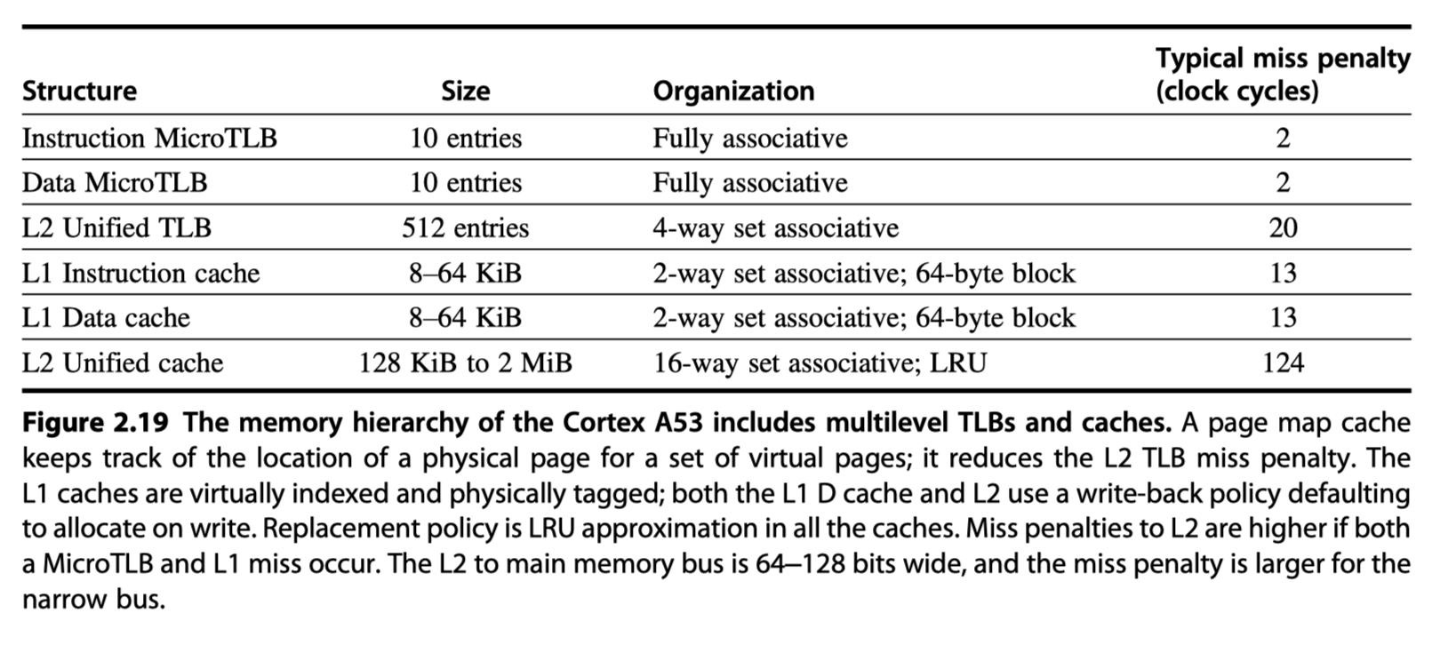
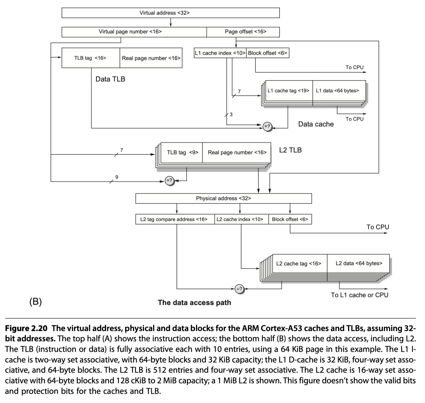
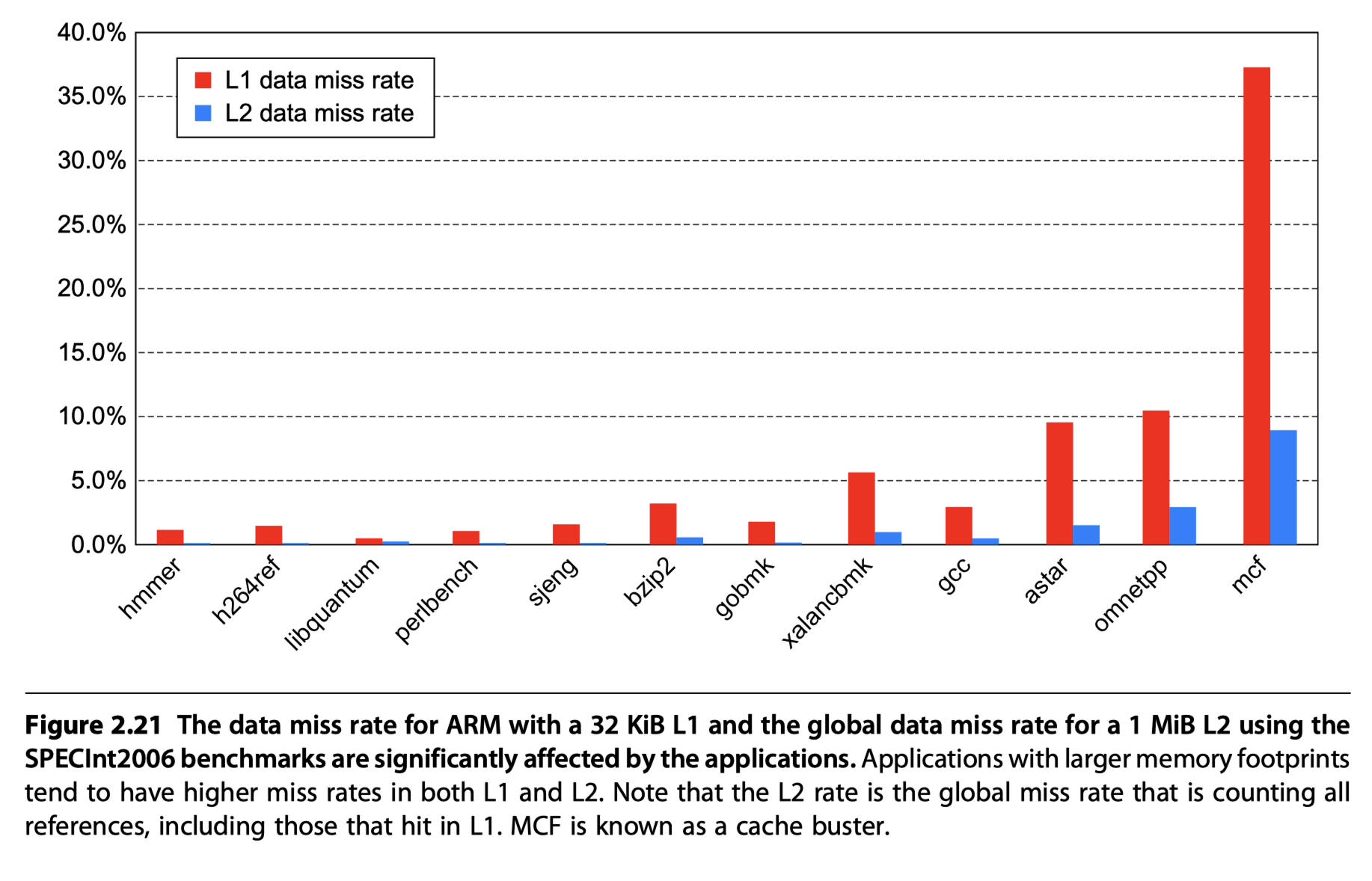
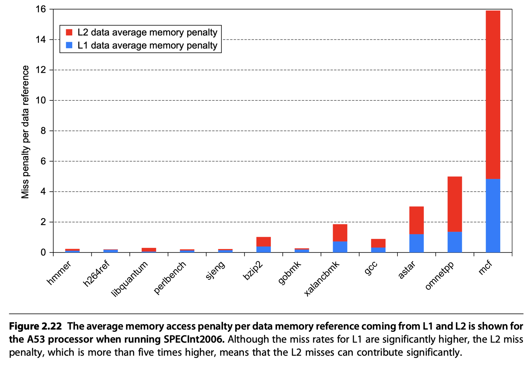
Performance of the Cortex-A53 Memory Hierarchy
- 32 KiB primary cache / 1 MiB L2 cache
- < 1% instruction cache miss rates for SpecInt2006 benchmarks
- Data cache miss and penalty?
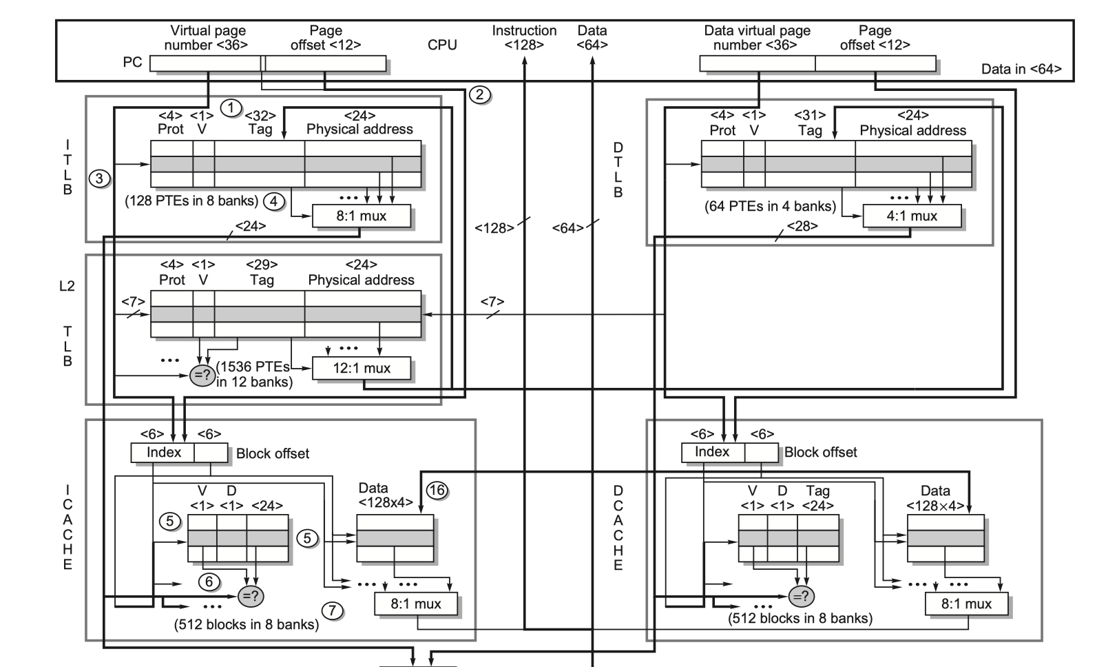
The Intel Core i7 6700
- 64-bit extension of the 80x86 architecture
- OoO execution processor
- Four 80x86 instructions per clock cycle @ up to 4.0 GHz
- Multiple issue
- Dynamically scheduled
- 16-stage pipeline
- Two simultaneous threads per processor = simultaneous multithreading
- Memory support
- Three memory channels
- DDR3-1066 (DIMM PC8500)
- Peak memory BW > 25 GB/s
- Virtual memory
- 48-bit virtual addresses
- 36-bit physical addresses
- Max physical memory = 36 GiB
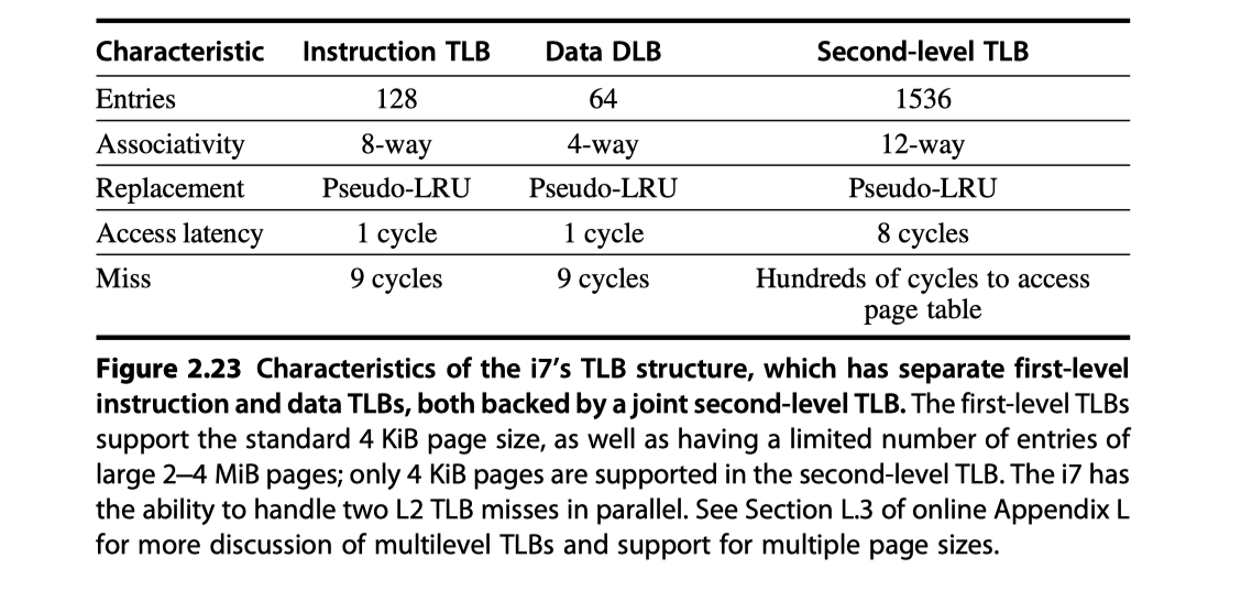
- Two-level TLB
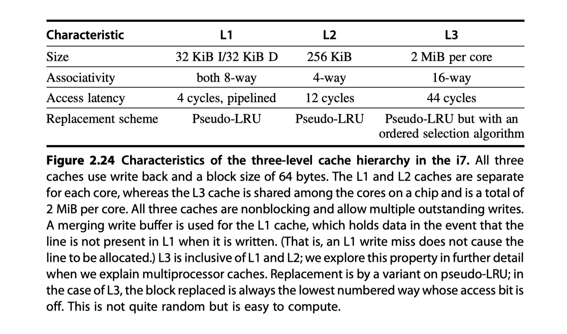
- L1 cache
- Virtually indexed
- Physically tagged
- L2 and L3
- Physically indexed
- L4
- Some version of i7 6700 use HBM as fourth level cache
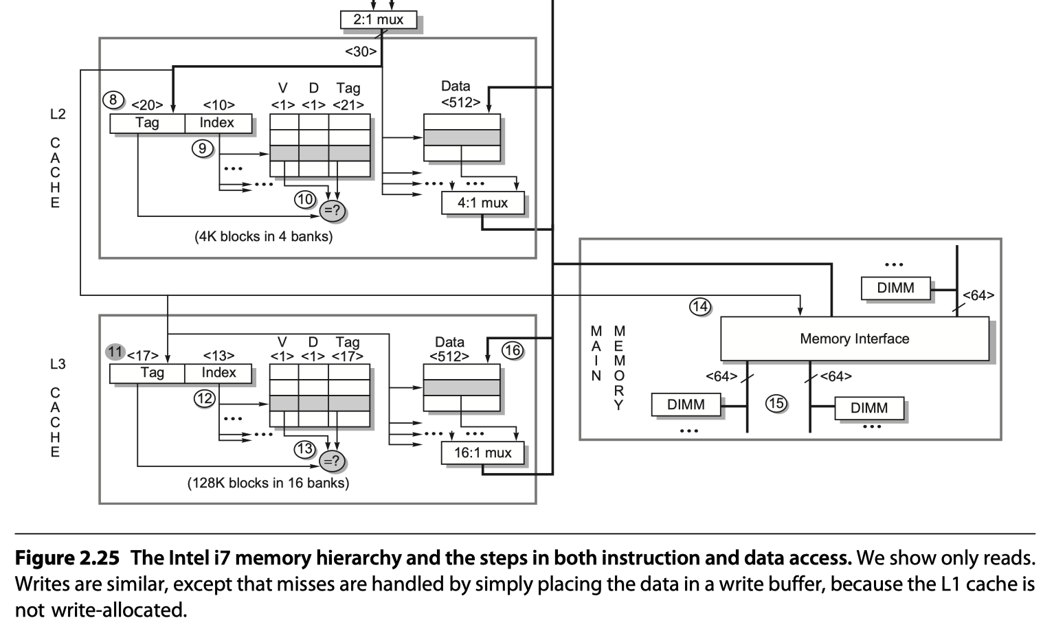
- Read page from 136 to for detailed explanation on
- the memory access steps and
- the performance related to
- Autonomous instruction fetch
- Speculation
- Instruction prefetch and data prefetch
Reference
- Chapter 2 in Computer Architecture A Quantitative Approach (6th) by Hennessy and Patterson (2017)
- Notebook: Computer Architecture Quantitive Approach
- Valsan, Prathap Kumar, Heechul Yun, and Farzad Farshchi. “Addressing isolation challenges of non-blocking caches for multicore real-time systems.” Real-Time Systems 53 (2017): 673-708.
- Belayneh, Samson, and David R. Kaeli. “A discussion on non-blocking/lockup-free caches.” ACM SIGARCH Computer Architecture News 24.3 (1996): 18-25.
- Nonblocking cache from MIT lecture by Arvind (with Asif Khan)
- Memory hierarchy lecture from CMPUT429/CMPE382 Winter 2001 by J. N. Amaral
- Loh and Hill, “EFFICIENTLY ENABLING CONVENTIONAL BLOCK SIZES FOR VERY LARGE DIESTACKED DRAM CACHES” (2011)
- Quresh and Loh, “Fundamental Latency Trade-offs in Architecting DRAM Cache” (2012)
- VMware Ballooning by FRANKBRIX
- Virtualization and Cloud Computing Lecture 6: Memory Virtualization Techniques by Mythili Vutukuru
- CS250 VLSI Systems Design Lecture 8: Memory by John Wawrzynek, Krste Asanovic, with John Lazzaro and Yunsup Lee (TA), CS250, UC Berkeley, Fall 2010
- EE241 - Spring 2011 Advanced Digital Integrated Circuits Lecture 9: SRAM
Notes Mentioning This Note
Table of Contents
- Memory Hierarchy Design
- Introduction
- Memory Technology and Optimization
-
Ten Advanced Optimizations of Cache Performance
- #1. Small and Simple First-Level Caches to Reduce Hit Time and Power
- #2. Way Prediction to Reduce Hit Time
- #3. Pipelined Access and Multibanked Caches to Increase Bandwidth
- #4. Opt.: Nonblocking Caches to Increase Cache Bandwidth
- #5. Critical Word First and Early Restart to Reduce Miss Penalty
- #6. Merging Write Buffer to Reduce Miss Penalty
- #7. Compiler Optimization to Reduce Miss Rate
- #8. Hardware Prefetching of Instructions and Data to Reduce Miss Penalty or Miss Rate
- #9. Compiler-Controlled Prefetching to Reduce Miss Penalty or Miss Rate
- #10. Using HBM to Extend the Memory Hierarchy
- Cache Optimization Summary
-
Virtual memory and Virtual Machines
- Protection via Virtual Memory
- Role of architecture for protection?
- Protection via Virtual Machines
- Requirements of a Virtual Machine Monitor
- Instruction Set Architecture Support for Virtual Machines
- Impact of Virtual Machines on Virtual Memory and I/O
- Extending the Instruction Set for Efficient Virtualization and Better Security
- An Example VMM: The Xem Virtual Machine
- Cross-Cutting Issues: The Design of Memory Hierarchies
- Putting It All Together: Memory Hierarchies in the ARM Cortex-A53 and Inter Core i7 6700
- Reference